
Datasheet


www.vishay.com
2
Document Number: 71738
S-83043-Rev. D, 22-Dec-08
Vishay Siliconix
Si7414DN
Notes
a. Pulse test; pulse width ≤ 300 µs, duty cycle ≤ 2 %.
b. Guaranteed by design, not subject to production testing.
Stresses beyond those listed under “Absolute Maximum Ratings” may cause permanent damage to the device. These are stress ratings only, and functional operation
of the device at these or any other conditions beyond those indicated in the operational sections of the specifications is not implied. Exposure to absolute maximum
rating conditions for extended periods may affect device reliability.
TYPICAL CHARACTERISTICS T
A
= 25 °C, unless otherwise noted
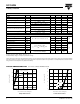
SPECIFICATIONS T
J
= 25 °C, unless otherwise noted
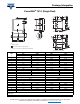
Parameter Symbol Test Conditions Min. Typ. Max. Unit
Static
Gate Threshold Voltage
V
GS(th)
V
DS
= V
GS
, I
D
= 250 µA
13V
Gate-Body Leakage
I
GSS
V
DS
= 0 V, V
GS
= ± 20 V
± 100 nA
Zero Gate Voltage Drain Current
I
DSS
V
DS
= 60 V, V
GS
= 0 V
1
µA
V
DS
= 60 V, V
GS
= 0 V, T
J
= 55 °C
5
On-State Drain Current
a
I
D(on)
V
DS
≥ 5 V, V
GS
= 10 V
30 A
Drain-Source On-State Resistance
a
R
DS(on)
V
GS
= 10 V, I
D
= 8.7 A
0.021 0.025
Ω
V
GS
= 4.5 V, I
D
= 7.3 A
0.030 0.036
Forward Transconductance
a
g
fs
V
DS
= 15 V, I
D
= 8.7 A
18 S
Diode Forward Voltage
a
V
SD
I
S
= 3.2 A, V
GS
= 0 V
0.75 1.2 V
Dynamic
b
Total Gate Charge
Q
g
V
DS
= 30 V, V
GS
= 10 V, I
D
= 8.7 A
16 25
nCGate-Source Charge
Q
gs
2.7
Gate-Drain Charge
Q
gd
4.4
Gate Resistance
R
g
1.0 Ω
Tur n - O n D e l ay Time
t
d(on)
V
DD
= 30 V, R
L
= 30 Ω
I
D
≅ 1 A, V
GEN
= 10 V, R
g
= 6 Ω
15 25
ns
Rise Time
t
r
12 20
Turn-Off DelayTime
t
d(off)
30 50
Fall Time
t
f
12 20
Source-Drain Reverse Recovery
Time
t
rr
I
F
= 3.2 A, dI/dt = 100 A/µs
45 90
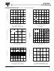
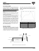
Output Characteristics
0
6
12
18
24
30
012345
V
GS
= 10 thru 5 V
3 V
V
DS
- Drain-to-Source Voltage (V)
Drain Current (A)I
D
-
4 V
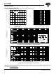
Transfer Characteristics
0
5
10
15
20
25
30
0 1234 5
25 °C
T
C
= 125 °C
- 55 °C
V
GS - Gate-to-Source Voltage (V)
Drain Current (A)I
D
-