
Datasheet

SFH636
www.vishay.com
Vishay Semiconductors
Rev. 1.8, 03-Aug-15
8
Document Number: 83681
For technical questions, contact: optocoupleranswers@vishay.com
THIS DOCUMENT IS SUBJECT TO CHANGE WITHOUT NOTICE. THE PRODUCTS DESCRIBED HEREIN AND THIS DOCUMENT
ARE SUBJECT TO SPECIFIC DISCLAIMERS, SET FORTH AT www.vishay.com/doc?91000
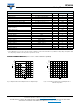
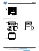
SMD-6, Option 9
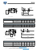
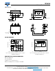
SOLDER PROFILES
Fig. 14 - Wave Soldering Double Wave Profile According to
J.STD-020 for DIP Devices
Fig. 15 - Lead (Pb)-free Reflow Solder Profile According to
J-STD-020 for SMD Devices
HANDLING AND STORAGE CONDITIONS
ESD level: HBM class 2
Floor life: unlimited
Conditions: T
amb
< 30 °C, RH < 85 %
Moisture sensitivity level 1, according to J-STD-020
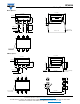
Pin one I.D.
65
4
123
R0.25
8.00 min.
11.05
1.52
1.78
2.54
0.76
8.60 ± 0.10
9.00 max.
0.90 min.
2.54 typ.
1.27 ± 0.10
3.55 ± 0.25
6.50 ± 0.25
7.62 typ.
10.05 max.
8.00 min.
0.50 min.
0.20 ± 0.10
Leads coplanarity
0.1 max.
0.25 ± 0.10
2 K/s
second
wave
first wave
wave
ca. 5 K/s
5 s
full line: typical
dotted line:
process limits
Time (s)
Temperature (°C)
300
250
200
150
100
50
0
050100
150 200 250
94 8626
Lead temperature
235 °C to
260 °C
100 °C to
130 °C
ca. 200 K/s
forced cooling
ca. 2 K/s
0
50
100
150
200
250
300
0 50 100 150 200 250 300
Time (s)
Temperature (°C)
240 °C
245 °C
max. 260 °C
max. 120 s
max. 100 s
217 °C
max. 30 s
max. ramp up 3 °C/s
max. ramp down 6 °C/s
19841
255 °C