
Datasheet
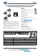

SFH636
www.vishay.com
Vishay Semiconductors
Rev. 1.8, 03-Aug-15
5
Document Number: 83681
For technical questions, contact: optocoupleranswers@vishay.com
THIS DOCUMENT IS SUBJECT TO CHANGE WITHOUT NOTICE. THE PRODUCTS DESCRIBED HEREIN AND THIS DOCUMENT
ARE SUBJECT TO SPECIFIC DISCLAIMERS, SET FORTH AT www.vishay.com/doc?91000
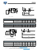
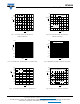
Fig. 7 - Permissible Total Power Dissipation vs.
Ambient Temperature
Fig. 8 - Forward Current of Emitting Diode vs. Forward Voltage
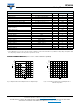
Fig. 9 - Small Signal Transfer Ratio vs. Forward Current
Fig. 10 - Current Transfer Ratio (Normalized) vs.
Ambient Temperature
Fig. 11 - Output Current (High) vs. Ambient Temperature
Fig. 12 - Delay Times vs. Ambient Temperature
100
120
mW
80
0 102030405060708090100
P
tot
T
A
60
40
20
0
Detector
Emitter
10
2
10
1
10
0
10
-1
0 1.2 1.3 1.4 1.5 1.6
I
F
/mA
VF/V
10
-2
10
-3
0.50
%
0.45
0.40
0.35
-60 -40 -20 0 20 40 60 ºC
100
T
A
0.30
0.25
0.20
0.15
0.10
0.05
0
V
CC
= 5.0 V
I
O
I
F
1.3
1.2
1.1
-60 -40 -20 0 20 40 60 ºC
100
T
A
1.0
0.9
0.8
0.7
0.6
I
F
= 16 mA,
V
O
= 0.4 V,
V
CC
= 5.0 V
NCTR
6N 135
6N 136
10
-6
10
-7
10
-8
10
-9
-60 -40 -20 0 20 40 60 ºC
100
I
OH
T
A
10
-10
10
-11
10
-12
V
0
= V
CC
= 5.0 V, I
F
= 0
1400
ns
1200
1000
-60 -40 -20 0 20 40 60 ºC
100
T
A
800
600
400
200
0
I
F
= 16 mA, V
CC
= 5.0 V,
R
L
= 4.1 kΩ, SFH636: R
L
= 1.9 kΩ
t
P
t
PLH
t
PHL
t
PLH
t
PHL
6N 135
6N 136