
Datasheet
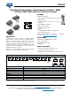

SFH636
www.vishay.com
Vishay Semiconductors
Rev. 1.8, 03-Aug-15
2
Document Number: 83681
For technical questions, contact: optocoupleranswers@vishay.com
THIS DOCUMENT IS SUBJECT TO CHANGE WITHOUT NOTICE. THE PRODUCTS DESCRIBED HEREIN AND THIS DOCUMENT
ARE SUBJECT TO SPECIFIC DISCLAIMERS, SET FORTH AT www.vishay.com/doc?91000
Note
• Stresses in excess of the absolute maximum ratings can cause permanent damage to the device. Functional operation of the device is not
implied at these or any other conditions in excess of those given in the operational sections of this document. Exposure to absolute
maximum ratings for extended periods of the time can adversely affect reliability.
Note
• Minimum and maximum values are testing requirements. Typical values are characteristics of the device and are the result of engineering
evaluation. Typical values are for information only and are not part of the testing requirements.
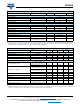
ABSOLUTE MAXIMUM RATINGS (T
amb
= 25 °C, unless otherwise specified)
PARAMETER CONDITIONS SYMBOL VALUE UNIT
INPUT
Reverse voltage V
R
3.0 V
DC forward current I
F
25 mA
Surge forward current t
P
≤ 1.0 μs, 300 pulses/s I
FSM
1.0 A
Power dissipation P
diss
45 mW
OUTPUT
Supply voltage V
S
-0.5 to +30 V
Output voltage V
O
-0.5 to +20 V
Output current I
O
8mA
Power dissipation P
diss
100 mW
COUPLER
Storage temperature range T
stg
-55 to +150 °C
Ambient temperature range T
amb
-55 to +100 °C
Junction temperature T
j
100 °C
Soldering temperature
Max. 10 s, dip soldering: distance
to seating plane ≥ 1.5 mm
T
sld
260 °C
ELECTRICAL CHARACTERISTICS (T
amb
= 0 °C to 70 °C unless otherwise specified, typ. values T
amb
= 25 °C)
PARAMETER TEST CONDITION SYMBOL MIN. TYP. MAX. UNIT
input
Forward voltage I
F
= 16 mA V
F
-1.51.8V
Reverse current V
R
= 3 V I
R
- 0.5 10 μA
Capacitance V
R
= 0 V, f = 1 MHz C
O
- 125 - pF
Thermal resistance R
thja
- 700 - K/W
output
Logic high supply current
I
F
= 0 V, V
O
(open),
V
CC
= 15 V, T
amb
= 25 °C
I
CCH
-0.011 μA
I
F
= 0 V, V
O
(open), V
CC
= 15 V I
CCH
-0.012 μA
Output current, output high
I
F
= 0 V, V
O
(open),
V
CC
= 5.5 V, T
amb
= 25 °C
I
OH
- 0.003 0.5 μA
I
F
= 0 V, V
O
(open),
V
CC
=15 V, T
amb
= 25 °C
I
OH
-0.011 μA
I
F
= 0 V, V
O
(open), V
CC
=15 V I
OH
-50μA
Collector emitter capacitance V
CE
= 5 V, f = 1 MHz C
CE
-3-pF
Thermal resistance R
thja
- 300 - K/W
coupler
Coupling capacitance C
C
-0.6-pF
Collector emitter saturation voltage
I
F
= 16 mA, I
O
= 2.4 mA,
V
CC
= 4.5 V; T
amb
= 25 °C
V
OL
-0.10.4V
Supply current, logic low I
F
= 16 mA, V
O
open, V
CC
= 15 V I
DD
-80-