
Datasheet


SFH618A, SFH6186
www.vishay.com
Vishay Semiconductors
Rev. 2.8, 29-Mar-18
2
Document Number: 83673
For technical questions, contact: optocoupleranswers@vishay.com
THIS DOCUMENT IS SUBJECT TO CHANGE WITHOUT NOTICE. THE PRODUCTS DESCRIBED HEREIN AND THIS DOCUMENT
ARE SUBJECT TO SPECIFIC DISCLAIMERS, SET FORTH AT www.vishay.com/doc?91000
Note
• Stresses in excess of the absolute maximum ratings can cause permanent damage to the device. Functional operation of the device is not
implied at these or any other conditions in excess of those given in the operational sections of this document. Exposure to absolute
maximum ratings for extended periods of the time can adversely affect reliability
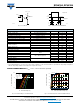
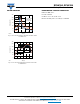
Fig. 1 - Permissible Power Dissipation vs. Ambient Temperature
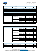
ABSOLUTE MAXIMUM RATINGS (T
amb
= 25 °C, unless otherwise specified)
PARAMETER TEST CONDITION SYMBOL VALUE UNIT
INPUT
Reverse voltage V
R
6V
Power dissipation P
diss
70 mW
Forward current I
F
60 mA
OUTPUT
Collector emitter voltage V
CEO
55 V
Emitter collector voltage V
ECO
7V
Collector current
I
C
50 mA
t
p
1 ms I
C
100 mA
Power dissipation P
diss
150 mW
COUPLER
Storage temperature range T
stg
-55 to +150 °C
Ambient temperature range T
amb
-55 to +100 °C
Junction temperature T
j
125 °C
Soldering temperature
max. 10 s, dip soldering distance
to seating plane 1.5 mm
T
sld
260 °C
10
100
1000
10000
0
50
100
150
200
0 255075100125
Axis Title
1st line
2nd line
2nd line
P
tot
- Total Power Dissipation (mW)
T
amb
- Ambient Temperature (°C)
LED
Detector