
Datasheet

S2A, S2B, S2D, S2G, S2J, S2K, S2M
www.vishay.com
Vishay General Semiconductor
Revision: 14-Aug-13
3
Document Number: 88712
For technical questions within your region: DiodesAmericas@vishay.com
, DiodesAsia@vishay.com, DiodesEurope@vishay.com
THIS DOCUMENT IS SUBJECT TO CHANGE WITHOUT NOTICE. THE PRODUCTS DESCRIBED HEREIN AND THIS DOCUMENT
ARE SUBJECT TO SPECIFIC DISCLAIMERS, SET FORTH AT www.vishay.com/doc?91000
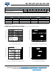
Fig. 5 - Typical Junction Capacitance Fig. 6 - Typical Transient Thermal Impedance
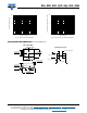
PACKAGE OUTLINE DIMENSIONS in inches (millimeters)
1
10
100
0.1 1 10 100
Junction Capacitance (pF)
Reverse Voltage (V)
10
100
1
0.01
1
100
0.1
10
t - Pulse Duration (s)
Transient Thermal Impedance (°C/W)
Cathode Band
DO-214AA (SMB)
0.086 (2.20)
0.077 (1.95)
0.155 (3.94)
0.130 (3.30)
0.180 (4.57)
0.160 (4.06)
0.012 (0.305)
0.006 (0.152)
0.008 (0.2)
0 (0)
0.220 (5.59)
0.205 (5.21)
0.060 (1.52)
0.030 (0.76)
0.096 (2.44)
0.084 (2.13)
Mounting Pad Layout
0.086 (2.18) MIN.
0.060 (1.52) MIN.
0.085 (2.159) MAX.
0.220 (5.59) REF.