
Datasheet

S1A, S1B, S1D, S1G, S1J, S1K, S1M
www.vishay.com
Vishay General Semiconductor
Revision: 25-Apr-14
3
Document Number: 88711
For technical questions within your region: DiodesAmericas@vishay.com
, DiodesAsia@vishay.com, DiodesEurope@vishay.com
THIS DOCUMENT IS SUBJECT TO CHANGE WITHOUT NOTICE. THE PRODUCTS DESCRIBED HEREIN AND THIS DOCUMENT
ARE SUBJECT TO SPECIFIC DISCLAIMERS, SET FORTH AT www.vishay.com/doc?91000
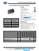
Fig. 3 - Typical Instantaneous Forward Characteristics
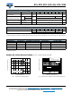
Fig. 4 - Typical Reverse Leakage Characteristics
Fig. 5 - Typical Junction Capacitance
Fig. 6 - Typical Transient Thermal Impedance
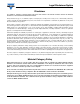
PACKAGE OUTLINE DIMENSIONS in inches (millimeters)
T
J
= 25 °C
Pulse Width = 300 µs
1 % Duty Cycle
0.4
100
1.6 2.00.8 1.2
Instantaneous Forward Voltage (V
)
Instantaneous Forward Current (A)
10
1
0.1
0.01
020 6040 10080
0.01
0.001
0.1
10
1
T
J
= 125 °C
T
J
= 25 °C
T
J
= 75 °C
Percent of Rated Peak Reverse Voltage (%)
Instantaneous Reverse Leakage
Current (µA)
Reverse Voltage (V)
Junction Capacitance (pF)
0.1 0.01 1 10 100
100
10
1
T
J
= 25 °C
f = 1.0 MHz
V
sig
= 50 mV
p-p
t - Pulse Duration (s)
Transient Thermal Impedance (°C/W)
0.1 0.01 1 10 100
100
1000
10
1
Units Mounted on
0.20" x 0.20" (5.0 mm x 5.0 mm)
x 0.5 Mil. Inches (0.013 mm)
Thick Copper Land Areas
S1A thru S1J
S1K, S1M
0.008 (0.203)
0.194 (4.93)
0.208 (5.28)
0.157 (3.99)
0.177 (4.50)
0.100 (2.54)
0.110 (2.79)
0.078 (1.98)
0.090 (2.29)
0.006 (0.152)
0.012 (0.305)
0.049 (1.25)
0.065 (1.65)
Cathode Band
0 (0)
DO-214AC (SMA)
Mounting Pad Layout
0.074 (1.88)
MAX.
0.208 (5.28)
REF.
0.066 (1.68)
MIN.
0.060 (1.52)
MIN.
0.030 (0.76)
0.060 (1.52)