
Datasheet

RS3A, RS3B, RS3D, RS3G, RS3J, RS3K
www.vishay.com
Vishay General Semiconductor
Revision: 25-Apr-14
3
Document Number: 88709
For technical questions within your region: DiodesAmericas@vishay.com
, DiodesAsia@vishay.com, DiodesEurope@vishay.com
THIS DOCUMENT IS SUBJECT TO CHANGE WITHOUT NOTICE. THE PRODUCTS DESCRIBED HEREIN AND THIS DOCUMENT
ARE SUBJECT TO SPECIFIC DISCLAIMERS, SET FORTH AT www.vishay.com/doc?91000
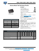
Fig. 3 - Typical Instantaneous Forward Characteristics
Fig. 4 - Typical Reverse Characteristics
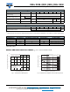
Fig. 5 - Typical Junction Capacitance
Fig. 6 - Typical Transient Thermal Impedance
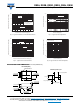
PACKAGE OUTLINE DIMENSIONS in inches (millimeters)
Instantaneous Forward Voltage (V)
Instantaneous Forward Current (A)
1.8
2.0
0.4
0.6
0.8
1.0
1.2
1.4
1
10
100
0.1
Pulse Width = 300 µs
1 % Duty Cycle
T
J
= 25 °C
1.6
T
J
= 125 °C
T
J
= - 40 °C
T
J
= 125 °C
T
J
= 25 °C
Percent of Rated Peak Reverse Voltage (%)
020406080 100
Instantaneous Reverse Current (µA)
100
10
1
0.1
0.01
T
J
= 75 °C
RS3A thr
u RS3G
100
10
1
1 10 100
Reverse Voltage (V)
Junction Capacitance (pF)
RS3J thru RS3K
0.01
0.1
1
10
100
0.1
1
10
100
Mounted on 0.20" x 0.27" (5 mm x 7 mm)
Copper Pad Areas
Transient Thermal Impedance (°C/W)
t - Pulse Duration (s)
Cathode Band
DO-214AB (SMC)
0.126 (3.20)
0.114 (2.90)
0.246 (6.22)
0.220 (5.59)
0.280 (7.11)
0.260 (6.60)
0.012 (0.305)
0.006 (0.152)
0.008 (0.2)
0 (0)
0.320 (8.13)
0.305 (7.75)
0.060 (1.52)
0.030 (0.76)
0.103 (2.62)
0.079 (2.06)
Mounting Pad Layout
0.126 (3.20) MIN.
0.060 (1.52) MIN.
0.185 (4.69) MAX.
0.320 (8.13) REF.