
Datasheet

RS1A, RS1B, RS1D, RS1G, RS1J, RS1K
www.vishay.com
Vishay General Semiconductor
Revision: 25-Apr-14
3
Document Number: 88707
For technical questions within your region: DiodesAmericas@vishay.com
, DiodesAsia@vishay.com, DiodesEurope@vishay.com
THIS DOCUMENT IS SUBJECT TO CHANGE WITHOUT NOTICE. THE PRODUCTS DESCRIBED HEREIN AND THIS DOCUMENT
ARE SUBJECT TO SPECIFIC DISCLAIMERS, SET FORTH AT www.vishay.com/doc?91000
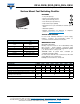
Fig. 3 - Typical Instantaneous Forward Characteristics
Fig. 4 - Typical Reverse Characteristics
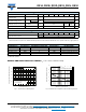
Fig. 5 - Typical Junction Capacitance
Fig. 6 - Typical Transient Thermal Impedance
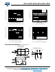
PACKAGE OUTLINE DIMENSIONS in inches (millimeters)
T
J
= 125 °C
T
J
= 25 °C
Pulse Width = 300 µs
1 % Duty Cycle
100
10
1
0.1
0.01
0.4 0.6 0.8 1.0 1.2 1.4 1.6 1.8
Instantaneous Forward Voltage (V)
Instantaneous Forward Current (A)
T
J
= 125 °C
T
J
= 100 °C
T
J
= 25 °C
Percent of Rated Peak Reverse Voltage (%)
0 20406080100
Instantaneous Reverse Current (µA)
100
10
1
0.1
0.01
RS1A thru RS1G
100
10
1
1 10 100
Reverse Voltage (V)
Junction Capacitance (pF)
T
J
= 25 °C
f = 1.0 MHz
V
sig
= 50 mV
p-p
RS1J thru RS1K
Mo
unted on 0.2" x 0.2" (5 mm x 5 mm)
Copper Pad Area
0.01 0.1 1 10
100
10
1
t - Pulse Duration (s)
Transient Thermal Impedance (°C/W)
0.008 (0.203)
0.194 (4.93)
0.208 (5.28)
0.157 (3.99)
0.177 (4.50)
0.100 (2.54)
0.110 (2.79)
0.078 (1.98)
0.090 (2.29)
0.006 (0.152)
0.012 (0.305)
0.049 (1.25)
0.065 (1.65)
Cathode Band
0 (0)
DO-214AC (SMA)
Mounting Pad Layout
0.074 (1.88)
MAX.
0.208 (5.28)
REF.
0.066 (1.68)
MIN.
0.060 (1.52)
MIN.
0.030 (0.76)
0.060 (1.52)