
Datasheet

NTCC200E4C90008
www.vishay.com
Vishay BCcomponents
Revision: 20-Mar-17
1
Document Number: 29168
For technical questions, contact: nlr@vishay.com
THIS DOCUMENT IS SUBJECT TO CHANGE WITHOUT NOTICE. THE PRODUCTS DESCRIBED HEREIN AND THIS DOCUMENT
ARE SUBJECT TO SPECIFIC DISCLAIMERS, SET FORTH AT www.vishay.com/doc?91000
Leadless NTC Thermistor Die intended for Wire Bonding
FEATURES
• Flat chip contacted top and bottom (Silver)
• Wide temperature range from -55 °C to +175 °C
• Specified at 100 °C for better temp. control
• Highly resistant to thermal shocks
• Ideal for wire bonding (aluminum or gold
depending on metalization type)
• Delivered on blister tape
• Material categorization:
for definitions of compliance please see
www.vishay.com/doc?99912
APPLICATIONS
• High temperature sensing, control and compensation.
E.g. IGBT modules (inverters in EV and HEV vehicles)
• IC and semiconductor protecting
• DC/AC power inverters and HIC overheat protecting
DESIGN-IN SUPPORT
For complete curve computation, please visit:
www.vishay.com/thermistors/ntc-curve-list/
MARKING
The thermistors have no marking and have electrode
termination design without orientation.
MOUNTING
The thermistors are primarily intended for wire bonding. The
parameters of the assembly process should be chosen in
accordance with the lead-wire material.
The mounting process should be in compliance with the
following guidelines and recommendations:
Die bonding:
• Gold electrode: silver epoxy gluing.
• Silver electrode: SAC reflow soldering - silver epoxy gluing
- nano silver sintering.
Cleaning:
• Detergent spraying.
• Ultrasonic cleaning is strictly prohibited.
Wire bonding:
• The gold electrode has been tested for gold wire bonding
with a wire diameter of 32 μm.
• The silver electrode has been tested for aluminum wire
bonding with a wire diameter of 300 μm.
Encapsulation:
• In order to preserve the characteristics of the bonded die
at long term an encapsulation is mandatory
.
• The encapsulation is defined by the customer. Silicon and
epoxy encapsulations have been tested.For
recommendations on compatible encapsulants contact
Vishay.
The behavior of the connected die is strongly depending on
the particular processing and application conditions and we
recommend to the users to test ,verify and validate for
themselves their particular application. Vishay will not
endorse any responsibility of an abnormal behavior of
components having been processed in non validated
executions.
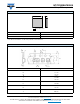
QUICK REFERENCE DATA
PARAMETER VALUE UNIT
Resistance value at 25 °C 5063
Resistance value at 100 °C 493.3
Tolerance on R
100
-value ± 5 %
B
25/85
-value 3435 K
Tolerance on B
25/85
-value ± 1 %
Operating temperature range -55 to +175 °C
Response time (63.2 %)
25 °C to 85 °C still air (for info)
3s
Dissipation factor in still air
(for info, non-mounted die)
3mW
Maximum power dissipation 50 mW
Weight 3 mg
ELECTRICAL DATA AND ORDERING INFORMATION
R
25
()
R
25
-TOL.
(± %)
B
25/85
(K)
B
25/85
-TOL.
(± %)
DESCRIPTION
SAP MATERIAL AND
ORDERING NUMBER
5063 7.43 3435 1
Bare die with top / bottom
silver termination
NTCC200E4C90008