
Datasheet
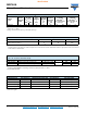
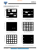
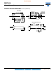
Table Of Contents
New Product
MSP5.0A
Vishay General Semiconductor
Document Number: 88487
Revision: 16-Jun-09
For technical questions within your region, please contact one of the following:
PDD-Americas@vishay.com
, PDD-Asia@vishay.com, PDD-Europe@vishay.com
www.vishay.com
3
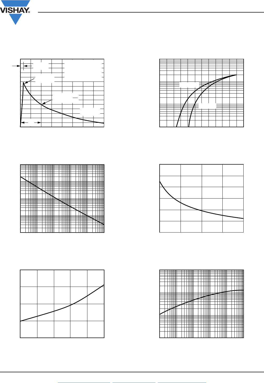
RATINGS AND CHARACTERISTICS CURVES
(T
A
= 25 °C unless otherwise noted)
Figure 1. Pulse Waveform
Figure 2. Peak Pulse Power Rating Curve
Figure 3. Relative Variation of Leakage Current vs.
Junction Temperature
0
0
50
100
150
1.0 2.0 3.0 4.0
t
r
= 10 µs
t
r
= 8 µs
t
d
= 1000 µs
t
d
= 20 µs
Peak Value
I
PPM
Half Value -
I
PPM
I
PP
2
t
d
I
PPM
- Peak Pulse Current, % I
RSM
t - Time (ms)
T
J
= 25 °C
Pulse Width (t
d
)
is defined as the Point
where the Peak Current
decays to 50 % of I
PPM
0.1
0.01
0.1
1
10
100
1 10 100 1000 10 000
P
PPM
- Peak Pulse Power (kW)
t
d
- Pulse Width (µs)
40
30
20
10
0
25 50 75 100 125 150
Reverse Leakage Current (µA)
T
J
- Junction Temperature (°C)
Figure 4. Typical Peak Forward Voltage Drop vs.
Peak Forward Current
Figure 5. Typical Junction Capacitance
Figure 6. Typical Transient Thermal Impedance
10
100
1
0.1
0.4 0.6 0.8 1.0 1.2 1.4 1.6
V
F
- Forward Voltage Drop (V)
Peak Forward Current (A)
T
J
= 150 °C
T
J
= 25 °C
200
300
400
500
600
700
800
10234
Reverse Voltage (V)
C
J
- Junction Capacitance (pF)
1000
100
10
1
0.10.01 1 10 100 1000
t - Pulse Duration (s)
Transient Thermal Impedance (°C/W)