
Datasheet

MSP3V3, MSP5.0A
www.vishay.com
Vishay General Semiconductor
Revision: 03-May-18
3
Document Number: 88486
For technical questions within your region: DiodesAmericas@vishay.com
, DiodesAsia@vishay.com, DiodesEurope@vishay.com
THIS DOCUMENT IS SUBJECT TO CHANGE WITHOUT NOTICE. THE PRODUCTS DESCRIBED HEREIN AND THIS DOCUMENT
ARE SUBJECT TO SPECIFIC DISCLAIMERS, SET FORTH AT www.vishay.com/doc?91000
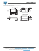
RATINGS AND CHARACTERISTICS CURVES (T
A
= 25 °C unless otherwise noted)
Fig. 1 - Pulse Waveform
Fig. 2 - Peak Pulse Power Rating Curve
Fig. 3 - Pulse Power or Current vs. Initial Junction Temperature
Fig. 4 - Typical Junction Capacitance
Fig. 5 - Power Dissipation Derating Curve
Fig. 6 - Typical Transient Thermal Impedance
0
0
50
100
150
1.0 2.0 3.0 4.0
t
r
= 10 μs
t
r
= 8 μs
t
d
= 1000 μs
t
d
= 20 μs
I
PPM
- Peak Pulse Current (% I
RSM
)
t - Time (ms)
t
d
Peak Value
I
PPM
Half Value -
I
PPM
I
PP
2
T
J
= 25 °C
Pulse Width (t
d
) is
dened as the Point
Where the Peak Current
decays to 50 % of I
PPM
0.1
0.01
0.1
1
10
100
1 10 100 1000 10 000
P
PPM
- Peak Pulse Power (kW)
t
d
- Pulse Width (μs)
0.24" x 0.24" (6.0 mm x 6.0 mm)
Copper Pad Areas
Non-Repetitive Pulse
Waveform Shown in Fig. 1
T
A
= 25 °C
50
75
100
25
0
0 50 75 100 125 175
Peak Pulse Power (P
PP
) or Current (I
PP
)
Derating in Percentage (%)
T
J
- Initial Temperature (°C)
25 150
100
1000
33.544.555.56
C
J
- Junction Capacitance (pF)
V
WM
- Reverse Stand-Off Voltage (V)
Measured at Stand-off
Voltage, V
WM
Measured at Zero Bias
T
J
= 25 °C
f = 1.0 MHz
V
sig
= 50 mV
p-p
0.0
0.2
0.4
0.6
0.8
1.0
1.2
500 100 150 175
Ambient Temperature (°C)
P
D
- Power Dissipation (W)
25 75 125
Mounted on Minimum
Recommende Pad Area
T
A
= T
M
, Mounted on
6.0 mm x 6.0 mm Copper Pad
1000
100
10
0.10.01 1 10 100 1000
t - Pulse Duration (s)
Transient Thermal Impedance (°C/W)
Junction to Ambient