
Datasheet

MSP3V3, MSP5.0A
www.vishay.com
Vishay General Semiconductor
Revision: 03-May-18
1
Document Number: 88486
For technical questions within your region: DiodesAmericas@vishay.com
, DiodesAsia@vishay.com, DiodesEurope@vishay.com
THIS DOCUMENT IS SUBJECT TO CHANGE WITHOUT NOTICE. THE PRODUCTS DESCRIBED HEREIN AND THIS DOCUMENT
ARE SUBJECT TO SPECIFIC DISCLAIMERS, SET FORTH AT www.vishay.com/doc?91000
Surface Mount TRANSZORB
®
Transient Voltage Suppressors
DESIGN SUPPORT TOOLS
FEATURES
• Very low profile - typical height of 0.65 mm
• Ideal for automated placement
• Oxide planar chip junction
• Uni-directional polarity only
• Peak pulse power: 150 W (10 μs/1000 μs)
• ESD capability: 15 kV (air), 8 kV (contact)
• Meets MSL level 1, per J-STD-020C, LF maximum peak
of 260 °C
• AEC-Q101 qualified
• Not recommended for PCB bottom side wave mounting
• Material categorization: for definitions of compliance
please see www.vishay.com/doc?99912
TYPICAL APPLICATIONS
Use in sensitive electronics protection against voltage
transients induced by inductive load switching and lighting
on ICs, MOSFET, industrial, and signal lines of sensor units
for protecting sensitive equipment against transient
overvoltages.
MECHANICAL DATA
Case: MicroSMP (DO-219AD)
Molding compound meets UL 94 V-0 flammability rating
Base P/N-M3 - halogen-free, RoHS-compliant, and
industrial grade
Base P/NHM3 - halogen-free, RoHS-compliant, and
automotive grade
Terminals: matte tin plated leads, solderable per
J-STD-002 and JESD 22-B102
M3 suffix meets JESD 201 class 2 whisker test, HM3 suffix
meets JESD 201 class 2 whisker test
Polarity: color band denotes the cathode end
Notes
(1)
Non-repetitive current pulse, per fig. 1
(2)
Mounted on 6.0 mm x 6.0 mm copper pads to each terminal
(3)
Mounted on minimum recommended pad layout
PRIMARY CHARACTERISTICS
V
WM
3.3 V to 5.0 V
V
BR
4.1 V to 7.07 V
P
PPM
150 W
T
J
max. 150 °C
Polarity Uni-directional
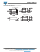
Package MicroSMP (DO-219AD)
MicroSMP (DO-219AD)
eSMP
®
Series
Top View
Bottom View
Cathode
Anode
click logo to get started
Available
Models
Available
MAXIMUM RATINGS (T
A
= 25 °C unless otherwise noted)
PARAMETER SYMBOL VALUE UNIT
Peak power dissipation with a 10/1000 μs waveform (fig. 1) P
PPM
(1)(2)
150 W
Peak pulse current with a 10/1000 μs waveform I
PPM
(1)
See next table A
Power dissipation T
M
= 120 °C P
D
(2)
1.0 W
Power dissipation T
A
= 25 °C P
D
(3)
0.5 W
Operating junction and storage temperature range T
J
, T
STG
-55 to +150 °C