PD - 95059 IRFPC60PbF • Lead-Free www.irf.
IRFPC60PbF 2 www.irf.
IRFPC60PbF www.irf.
IRFPC60PbF 4 www.irf.
IRFPC60PbF www.irf.
IRFPC60PbF 6 www.irf.
IRFPC60PbF Peak Diode Recovery dv/dt Test Circuit Circuit Layout Considerations • Low Stray Inductance • Ground Plane • Low Leakage Inductance Current Transformer + + - - + • dv/dt controlled by RG • ISD controlled by Duty Factor "D" • D.U.T. - Device Under Test + - * Reverse Polarity for P-Channel ** Use P-Channel Driver for P-Channel Measurements Driver Gate Drive P.W. D= Period P.W. Period VGS=10V D.U.T. ISD Waveform Reverse Recovery Current Body Diode Forward Current di/dt D.U.T.
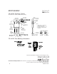
IRFPC60PbF TO-247AC Package Outline Dimensions are shown in millimeters (inches) -D- 3.65 (.143) 3.55 (.140) 15.90 (.626) 15.30 (.602) -B- 0.25 (.010) M D B M -A5.50 (.217) 20.30 (.800) 19.70 (.775) 2X 1 2 5.30 (.209) 4.70 (.185) 2.50 (.089) 1.50 (.059) 4 NOTES: 5.50 (.217) 4.50 (.177) 1 DIMENSIONING & TOLERANCING PER ANSI Y14.5M, 1982. 2 CONTROLLING DIMENSION : INCH. 3 CONFORMS TO JEDEC OUTLINE TO-247-AC. 3 -C- 14.80 (.583) 14.20 (.559) 2.40 (.094) 2.00 (.079) 2X 5.45 (.215) 2X 4.30 (.