
Datasheet

IRFB11N5OA
6 www.irf.com
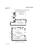
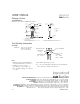
Q
G
Q
GS
Q
GD
V
G
Charge
D.U.T.
V
DS
I
D
I
G
3mA
V
GS
.3µF
50KΩ
.2µF
12V
Current Regulator
Same Type as D.U.T.
Current Sampling Resistors
+
-
10 V
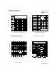
Fig 13b. Gate Charge Test Circuit
Fig 13a. Basic Gate Charge Waveform
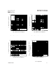
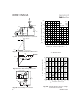
Fig 12c. Maximum Avalanche Energy
Vs. Drain Current
Fig 12b. Unclamped Inductive Waveforms
Fig 12a. Unclamped Inductive Test Circuit
t
p
V
(BR)DSS
I
AS
R
G
I
AS
0.01
Ω
t
p
D.U.T
L
V
DS
+
-
V
DD
DRIVER
A
15V
20V
Fig 12d. Typical Drain-to-Source Voltage
Vs. Avalanche Current
580
600
620
640
660
0.0 1.0 2.0 3.0 4.0 5.0 6.0 7.0
A
DSav
av
I , Avalanche Current
(
A
)
V , Avalanche Voltage (V)
25 50 75 100 125 150
0
100
200
300
400
500
600
Starting T , Junction Temperature ( C)
E , Single Pulse Avalanche Energy (mJ)
J
AS
°
I
D
TOP
BOTTOM
4.9A
7.0A
11A