
Datasheet

IRFB11N5OA
2 www.irf.com
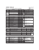
Parameter Min. Typ. Max. Units Conditions
g
fs
Forward Transconductance 6.1 ––– ––– S V
DS
= 50V, I
D
= 6.6A
Q
g
Total Gate Charge ––– ––– 52 I
D
= 11A
Q
gs
Gate-to-Source Charge ––– ––– 13 nC V
DS
= 400V
Q
gd
Gate-to-Drain ("Miller") Charge ––– ––– 18 V
GS
= 10V, See Fig. 6 and 13
t
d(on)
Turn-On Delay Time ––– 14 ––– V
DD
= 250V
t
r
Rise Time ––– 35 ––– I
D
= 11A
t
d(off)
Turn-Off Delay Time ––– 32 ––– R
G
= 9.1Ω
t
f
Fall Time ––– 28 ––– R
D
= 22Ω,See Fig. 10
C
iss
Input Capacitance ––– 1423 ––– V
GS
= 0V
C
oss
Output Capacitance ––– 208 ––– V
DS
= 25V
C
rss
Reverse Transfer Capacitance ––– 8.1 ––– pF ƒ = 1.0MHz, See Fig. 5
C
oss
Output Capacitance ––– 2000 ––– V
GS
= 0V, V
DS
= 1.0V, ƒ = 1.0MHz
C
oss
Output Capacitance ––– 55 ––– V
GS
= 0V, V
DS
= 400V, ƒ = 1.0MHz
C
oss
eff. Effective Output Capacitance ––– 97 ––– V
GS
= 0V, V
DS
= 0V to 400V
Parameter Min. Typ. Max. Units Conditions
V
(BR)DSS
Drain-to-Source Breakdown Voltage 500 ––– ––– V V
GS
= 0V, I
D
= 250µA
R
DS(on)
Static Drain-to-Source On-Resistance ––– ––– 0.52 Ω V
GS
= 10V, I
D
= 6.6A
V
GS(th)
Gate Threshold Voltage 2.0 ––– 4.0 V V
DS
= V
GS
, I
D
= 250µA
––– ––– 25
µA
V
DS
= 500V, V
GS
= 0V
––– ––– 250 V
DS
= 400V, V
GS
= 0V, T
J
= 150°C
Gate-to-Source Forward Leakage ––– ––– 100 V
GS
= 30V
Gate-to-Source Reverse Leakage ––– ––– -100
nA
V
GS
= -30V
Static @ T
J
= 25°C (unless otherwise specified)
I
GSS
I
DSS
Drain-to-Source Leakage Current
Dynamic @ T
J
= 25°C (unless otherwise specified)
ns
Parameter Typ. Max. Units
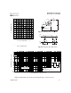
E
AS
Single Pulse Avalanche Energy ––– 275 mJ
I
AR
Avalanche Current ––– 11 A
E
AR
Repetitive Avalanche Energy ––– 17 mJ
Avalanche Characteristics
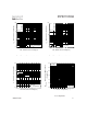
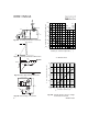
S
D
G
Parameter Min. Typ. Max. Units Conditions
I
S
Continuous Source Current MOSFET symbol
(Body Diode)
––– –––
showing the
I
SM
Pulsed Source Current integral reverse
(Body Diode)
––– –––
p-n junction diode.
V
SD
Diode Forward Voltage ––– ––– 1.5 V T
J
= 25°C, I
S
= 11A, V
GS
= 0V
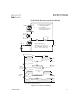
t
rr
Reverse Recovery Time ––– 510 770 ns T
J
= 25°C, I
F
= 11A
Q
rr
Reverse RecoveryCharge ––– 3.4 5.1 µC di/dt = 100A/µs
t
on
Forward Turn-On Time Intrinsic turn-on time is negligible (turn-on is dominated by L
S
+L
D
)
Diode Characteristics
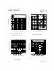
11
44
A
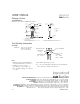
Parameter Typ. Max. Units
R
θJC
Junction-to-Case ––– 0.75
R
θCS
Case-to-Sink, Flat, Greased Surface 0.50 ––– °C/W
R
θJA
Junction-to-Ambient ––– 62
Thermal Resistance