
Datasheet


IRF9610S, SiHF9610S
www.vishay.com
Vishay Siliconix
S12-1558-Rev. D, 02-Jul-12
2
Document Number: 91081
For technical questions, contact: hvm@vishay.com
THIS DOCUMENT IS SUBJECT TO CHANGE WITHOUT NOTICE. THE PRODUCTS DESCRIBED HEREIN AND THIS DOCUMENT
ARE SUBJECT TO SPECIFIC DISCLAIMERS, SET FORTH AT www.vishay.com/doc?91000
Note
a. When mounted on 1" square PCB (FR-4 or G-10 material).
Notes
a. Repetitive rating; pulse width limited by maximum junction temperature (see fig. 5).
b. Pulse width 300 μs; duty cycle 2 %.
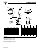
THERMAL RESISTANCE RATINGS
PARAMETER SYMBOL TYP. MAX. UNIT
Maximum Junction-to-Ambient R
thJA
-62
°C/W
Maximum Junction-to-Ambient
(PCB Mount)
a
R
thJA
-40
Maximum Junction-to-Case (Drain) R
thJC
-6.4
SPECIFICATIONS (T
J
= 25 °C, unless otherwise noted)
PARAMETER SYMBOL TEST CONDITIONS MIN. TYP. MAX. UNIT
Static
Drain-Source Breakdown Voltage V
DS
V
GS
= 0, I
D
= - 250 μA - 200 - - V
V
DS
Temperature Coefficient V
DS
/T
J
Reference to 25 °C, I
D
= - 1 mA - - 0.23 - V/°C
Gate-Source Threshold Voltage V
GS(th)
V
DS
= V
GS
, I
D
= - 250 μA - 2 - - 4 V
Gate-Source Leakage I
GSS
V
GS
= ± 20 V - - ± 100 nA
Zero Gate Voltage Drain Current I
DSS
V
DS
= - 200 V, V
GS
= 0 V - - - 100
μA
V
DS
= - 160 V, V
GS
= 0 V, T
J
= 125 °C - - - 500
Drain-Source On-State Resistance R
DS(on)
V
GS
= - 10 V I
D
= - 0.90 A
b
--3
Forward Transconductance g
fs
V
DS
= - 50 V, I
D
= - 0.90 A
b
0.90 - - S
Dynamic
Input Capacitance C
iss
V
GS
= 0 V,
V
DS
= - 25 V,
f = 1 MHz, see fig. 10
- 170 -
pFOutput Capacitance C
oss
-50-
Reverse Transfer Capacitance C
rss
-15-
Total Gate Charge Q
g
V
GS
= - 10 V
I
D
= - 3.5 A, V
DS
= - 160 V,
see fig. 11 and 18
b
--11
nC Gate-Source Charge Q
gs
--7
Gate-Drain Charge Q
gd
--4
Turn-On Delay Time t
d(on)
V
DD
= - 100 V, I
D
= - 0.90 A,
R
G
= 50 , R
D
= 110 , see fig. 17
b
-8-
ns
Rise Time t
r
-15-
Turn-Off Delay Time t
d(off)
-1-
Fall Time t
f
-8-
Internal Drain Inductance L
D
Between lead,
6 mm (0.25") from
package and center of
die contact
-4.5-
nH
Internal Source Inductance L
S
-7.5-
Drain-Source Body Diode Characteristics
Continuous Source-Drain Diode Current I
S
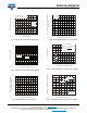
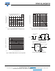
MOSFET symbol
showing the
integral reverse
p - n junction diode
--- 1.8
A
Pulsed Diode Forward Current
a
I
SM
--- 7
Body Diode Voltage V
SD
T
J
= 25 °C, I
S
= - 1.8 A, V
GS
= 0 V
b
--- 5.8V
Body Diode Reverse Recovery Time t
rr
T
J
= 25 °C, I
F
= - 1.8 A, dI/dt = 100 A/μs
b
- 240 360 ns
Body Diode Reverse Recovery Charge Q
rr
-1.72.6μC
Forward Turn-On Time t
on
Intrinsic turn-on time is negligible (turn-on is dominated by L
S
and L
D
)
D
S
G
S
D
G