
Datasheet


IRF9610S, SiHF9610S
www.vishay.com
Vishay Siliconix
S12-1558-Rev. D, 02-Jul-12
1
Document Number: 91081
For technical questions, contact: hvm@vishay.com
THIS DOCUMENT IS SUBJECT TO CHANGE WITHOUT NOTICE. THE PRODUCTS DESCRIBED HEREIN AND THIS DOCUMENT
ARE SUBJECT TO SPECIFIC DISCLAIMERS, SET FORTH AT www.vishay.com/doc?91000
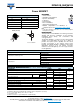
Power MOSFET
FEATURES
• Surface Mount
• Available in Tape and Reel
• Dynamic dV/dt Rating
•P-Channel
• Fast Switching
• Ease of Paralleling
• Simple Drive Requirements
• Material categorization: For definitions of
compliance please see www.vishay.com/doc?99912
Note
* Lead (Pb)-containing terminations are not RoHS-compliant.
Exemptions may apply.
DESCRIPTION
Third generation Power MOSFETs from Vishay provide the
designer with the best combination of fast switching,
ruggedized device design, low on-resistance and
cost-effectiveness.
The D
2
PAK (TO-263) is a surface mount power package
capable of accommodating die sizes up to HEX-4. It
provides the highest power capability and the lowest
possible on-resistance in any existing surface mount
package. The D
2
PAK (TO-263) is suitable for high current
applications because of its low internal connection
resistance and can dissipate up to 2 W in a typical surface
mount application.
Notes
a. Repetitive rating; pulse width limited by maximum junction temperature (see fig. 5).
b. I
SD
- 1.8 A, dI/dt 70 A/μs, V
DD
V
DS
, T
J
150 °C.
c. 1.6 mm from case.
d. When mounted on 1" square PCB (FR-4 or G-10 material).
PRODUCT SUMMARY
V
DS
(V) - 200
R
DS(on)
()V
GS
= - 10 V 3
Q
g
(Max.) (nC) 11
Q
gs
(nC) 7
Q
gd
(nC) 4
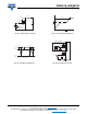
Configuration Single
S
G
D
P-Channel MOSFET
D
2
PAK (TO-263)
G
D
S
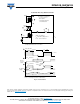
ORDERING INFORMATION
Package D
2
PAK (TO-263)
Lead (Pb)-free and Halogen-free
SiHF9610S-GE3
SiHF9610STRR-GE3
SiHF9610STRL-GE3
Lead (Pb)-free
IRF9610SPbF
SiHF9610S-E3
IRF9610STRRPbF
IRF9610STRLPbF
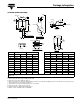
ABSOLUTE MAXIMUM RATINGS (T
C
= 25 °C, unless otherwise noted)
PARAMETER SYMBOL LIMIT UNIT
Drain-Source Voltage V
DS
- 200
V
Gate-Source Voltage V
GS
± 20
Continuous Drain Current V
GS
at - 10 V
T
C
= 25 °C
I
D
- 1.8
AT
C
= 100 °C - 1
Pulsed Drain Current
a
I
DM
- 7
Linear Derating Factor 0.16
W/°C
Linear Derating Factor (PCB Mount)
d
0.025
Maximum Power Dissipation T
C
= 25 °C
P
D
20
W
Maximum Power Dissipation (PCB Mount)
d
T
A
= 25 °C 3
Peak Diode Recovery dV/dt
b
dV/dt - 5 V/ns
Operating Junction and Storage Temperature Range T
J
, T
stg
- 55 to + 150
°C
Soldering Recommendations (Peak Temperature) for 10 s 300
c