
Datasheet
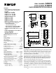


5–1
FEATURES
• Identical Channel to Channel Footprint
• Current Transfer Ratio (CTR) Range at
I
F
=10 mA
ILD/Q615-1: 40 – 80% Min.
ILD/Q615-2: 63 – 125% Min.
ILD/Q615-3: 100 – 200% Min.
ILD/Q615-4: 160 – 320% Min.
• Guaranteed CTR at I
F
=1 mA
ILD/Q615-1: 13% Min.
ILD/Q615-2: 22% Min.
ILD/Q615-3: 34% Min.
ILD/Q615-4: 56% Min.
• High Collector-Emitter Voltage BV
CEO
=70 V
• Dual and Quad Packages Feature:
- Reduced Board Space
- Lower Pin and Parts Count
- Better Channel to Channel CTR Match
- Improved Common Mode Rejection
• Field-Effect Stable by TRIOS (TR
ansparent
IO
n
S
hield
)
• Isolation Test Voltage from Double Molded
Package, 5300 VAC
RMS
• UL Approval #E52744
• VDE #0884 Available with Option 1
Maximum Ratings
(Each Channel)
Emitter
Reverse Voltage................................................ 6 V
Forward Current........................................... 60 mA
Surge Current .................................................1.5 A
Power Dissipation ......................................100 mW
Derate Linearly from 25
°
C ...................1.33 mW/
°
C
Detector
Collector-Emitter Reverse Voltage .................. 70 V
Emitter-Collector Reverse Voltage .................... 7 V
Collector Current.......................................... 50 mA
Collector Current (t <1 ms) .........................100 mA
Power Dissipation ......................................150 mW
Derate Linearly from 25
°
C........................ 2 mW/
°
C
Package
Storage Temperature................... –55
°
C to +150
°
C
Operating Temperature............... –55
°
C to +100
°
C
Junction Temperature....................................100
°
C
Soldering Temperature
(2 mm distance from case bottom)...........260
°
C
Package Power Dissipation, ILD615..........400 mW
Derate Linearly from 25
°
C..................5.33 mW/
°
C
Package Power Dissipation, ILQ615 .........500 mW
Derate Linearly from 25
°
C................. 6.67 mW/
°
C
Isolation Test Voltage (t=1 sec.)........5300 VAC
RMS
Creepage............................................... 7 mm min.
Clearance............................................... 7 mm min.
Isolation Resistance
V
IO
=500 V, T
A
=25
°
C...............................
≥
10
12
Ω
V
IO
=500 V, T
A
=100
°
C.............................
≥
10
11
Ω
DESCRIPTION
The ILD/Q615 are multi-channel phototransistor optocouplers that use GaAs
IRLED emitters and high gain NPN phototransistors. These devices are con-
structed using over/under leadframe optical coupling and double molded
insulation technology resulting a Withstand Test Voltage of 7500 VAC
PEAK
and a Working Voltage of 1700 VAC
RMS
.
The binned min./max. and linear CTR characteristics combined with the
TRIOS (TRansparent IOn Shield) field-effect process make these devices
well suited for DC or AC voltage detection. Eliminating the phototransistor
base connection provides added electrical noise immunity from the tran-
sients found in many industrial control environments.
Because of guaranteed maximum non-saturated and saturated switching
characteristics, the ILD/Q615 can be used in medium speed data I/O and
control systems. The binned min./max. CTR specification allow easy worst
case interface calculations for both level detection and switching applica-
tions. Interfacing with a CMOS logic is enhanced by the guaranteed CTR at
an I
F
=1 mA.
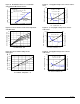
See Appnote 45, “How to Use Optocoupler Normalized Curves.”
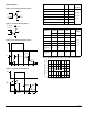
Dimensions in inches (mm)
.268 (6.81)
.255 (6.48)
34
65
.390 (9.91)
.379 (9.63)
.045 (1.14)
.030 (.76)
4°
Typ.
.100 (2.54) Typ.
10° Typ.
3°–9°
.305 Typ.
(7.75) Typ.
.022 (.56)
.018 (.46)
.012 (.30)
.008 (.20)
.135 (3.43)
.115 (2.92)
12
87
Pin One I.D.
.150 (3.81)
.130 (3.30)
.040 (1.02)
.030 (.76 )
1
2
3
4
8
7
6
5
Collector
Emitter
Collector
Emitter
Anode
Cathode
Anode
Cathode
Collecto
r
Emitter
Collecto
r
Emitter
Collecto
r
Emitter
Collecto
r
Emitter
Anode
Cathode
Anode
Cathode
Anode
Cathode
Anode
Cathode
1
2
3
4
5
6
7
8
16
15
14
13
12
11
10
9
.
268 (6.81)
.
255 (6.48)
.790 (20.07)
.779 (19.77 )
.045 (1.14)
.030 (.76)
4°
Typ.
.100 (2.54) Typ.
10° Typ.
3°–9°
.305 Typ.
(7.75) Typ.
.022 (.56)
.018 (.46)
.012 (.30)
.008 (.20)
.135 (3.43
)
.115 (2.92
)
Pin
One
I.D.
.150 (3.81)
.130 (3.30)
.040 (1.02)
.030 (.76 )
DUAL CHANNEL
ILD615
QUAD CHANNEL
ILQ615
PHOTOTRANSISTOR OPTOCOUPLER