
Datasheet


www.vishay.com
2
Document Number 83621
Rev. 1.4, 20-Apr-04
VISHAY
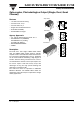
IL30/ 31/ 55/ ILD30/ 31/ 55/ ILQ30/ 31/ 55
Vishay Semiconductors
Order Information
For additional information on the available options refer to
Option Information.
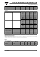
Absolute Maximum Ratings
T
amb
= 25 °C, unless otherwise specified
Stresses in excess of the absolute Maximum Ratings can cause permanent damage to the device. Functional operation of the device is
not implied at these or any other conditions in excess of those given in the operational sections of this document. Exposure to absolute
Maximum Rating for extended periods of the time can adversely affect reliability.
Input
(each channel)
Output
Part Remarks
IL30 CTR > 100 %, Single Channel DIP-6
IL31 CTR > 200 %, Single Channel DIP-6
IL55 CTR > 100 %, Single Channel DIP-6
ILD30 CTR > 100 %, Dual Channel DIP-8
ILD31 CTR > 200 %, Dual Channel DIP-8
ILD55 CTR > 100 %, Dual Channel DIP-8
ILQ30 CTR > 100 %, Quad Channel DIP-16
ILQ31 CTR > 200 %, Quad Channel DIP-16
ILQ55 CTR > 100 %, Quad Channel DIP-16
IL55-X009 CTR > 100 %, Single Channel SMD-6 (option 9)
ILD30-X009 CTR > 100 %, Dual Channel SMD-8 (option 9)
ILD31-X007 CTR > 200 %, Dual Channel SMD-8 (option 7)
ILD31-X009 CTR > 200 %, Dual Channel SMD-8 (option 9)
ILD55-X007 CTR > 100 %, Dual Channel SMD-8 (option 7)
ILD55-X009 CTR > 100 %, Dual Channel SMD-8 (option 9)
ILQ30-X009 CTR > 100 %, Quad Channel SMD-16 (option 9)
ILQ55-X007 CTR > 100 %, Quad Channel SMD-16 (option 7)
ILQ55-X009 CTR > 100 %, Quad Channel SMD-16 (option 9)
Parameter Test condition Symbol Value Unit
Peak reverse voltage V
RM
3.0 V
Forward continuous current I
F
60 mA
Power dissipation P
diss
100 mW
Derate linearly from 25 °C 1.33 mW/°C
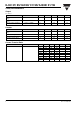
Parameter Test condition Part Symbol Value Unit
Collector-emitter breakdown voltage IL30 BV
CEO
30 V
ILD30 BV
CEO
30 V
ILQ30 BV
CEO
30 V
IL55 BV
CEO
55 V
ILD55 BV
CEO
55 V
ILD55 BV
CEO
55 V