
Datasheet

ILD217T
www.vishay.com
Vishay Semiconductors
Rev. 1.0, 23-Jul-14
2
Document Number: 84268
For technical questions, contact: optocoupleranswers@vishay.com
THIS DOCUMENT IS SUBJECT TO CHANGE WITHOUT NOTICE. THE PRODUCTS DESCRIBED HEREIN AND THIS DOCUMENT
ARE SUBJECT TO SPECIFIC DISCLAIMERS, SET FORTH AT www.vishay.com/doc?91000
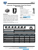
Notes
• Stresses in excess of the absolute maximum ratings can cause permanent damage to the device. Functional operation of the device is not
implied at these or any other conditions in excess of those given in the operational sections of this document. Exposure to absolute
maximum ratings for extended periods of the time can adversely affect reliability.
(1)
Refer to reflow profile for soldering conditions for surface mounted devices.
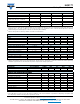
Note
• Minimum and maximum values were tested requirements. Typical values are characteristics of the device and are the result of engineering
evaluations. Typical values are for information only and are not part of the testing requirements.
Note
• As per IEC 60747-5-5, §7.4.3.8.2, this optocoupler is suitable for “safe electrical insulation” only within the safety ratings. Compliance with
the safety ratings shall be ensured by means of protective circuits.
COUPLER
Isolation test voltage t = 1 s V
ISO
4000 V
RMS
Total package dissipation ambient
(2 LEDs and 2 detectors, 2 channels)
P
tot
350 mW
Storage temperature T
stg
-55 to +150 °C
Operating temperature T
amb
-55 to +100 °C
Soldering time from 260 °C
(1)
T
sld
10 s
ELECTRICAL CHARACTERISTICS (T
amb
= 25 °C, unless otherwise specified)
PARAMETER TEST CONDITION SYMBOL MIN. TYP. MAX. UNIT
INPUT
Forward voltage I
F
= 10 mA V
F
1.2 1.55 V
Reverse current V
R
= 6 V I
R
0.1 100 μA
Capacitance V
R
= 0 V C
O
25 pF
OUTPUT
Collector emitter breakdown voltage I
C
= 10 μA BV
CEO
70 V
Emitter collector breakdown voltage I
E
= 10 μA BV
ECO
7V
Collector emitter leakage current V
CE
= 10 V, I
F
= 0 A I
CEO
550nA
Collector emitter capacitance V
CE
= 0 V C
CE
10 pF
COUPLER
Collector emitter saturation voltage I
F
= 10 mA, I
C
= 2.5 mA V
CEsat
0.4 V
Capacitance (input to output) C
IO
0.5 pF
Resistance (input to output) R
IO
100 GΩ
CURRENT TRANSFER RATIO (T
amb
= 25 °C, unless otherwise specified)
PARAMETER TEST CONDITION SYMBOL MIN. TYP. MAX. UNIT
I
C
/I
F
V
CE
= 5 V, I
F
= 1 mA CTR 100 120 %
SAFETY AND INSULATION RATINGS
PARAMETER TEST CONDITION SYMBOL MIN. TYP. MAX. UNIT
Climatic classification according to IEC 68 part 1 55/100/21
Comparative tracking index CTI 175 399
V
IOTM
6000 V
V
IORM
560 V
P
SO
350 mW
I
SI
150 mA
T
SI
165 °C
Creepage distance 4mm
Clearance distance 4mm
Insulation thickness 0.2 mm
ABSOLUTE MAXIMUM RATINGS (T
amb
= 25 °C, unless otherwise specified)
PARAMETER TEST CONDITION SYMBOL VALUE UNIT