
Datasheet

ICTE5 thru ICTE18C, 1N6373 thru 1N6386
www.vishay.com
Vishay General Semiconductor
Revision: 18-Sep-12
3
Document Number: 88356
For technical questions within your region: DiodesAmericas@vishay.com
, DiodesAsia@vishay.com, DiodesEurope@vishay.com
THIS DOCUMENT IS SUBJECT TO CHANGE WITHOUT NOTICE. THE PRODUCTS DESCRIBED HEREIN AND THIS DOCUMENT
ARE SUBJECT TO SPECIFIC DISCLAIMERS, SET FORTH AT www.vishay.com/doc?91000
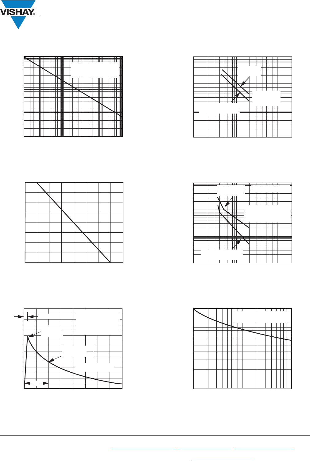
RATINGS AND CHARACTERISTICS CURVES (T
A
= 25 °C unless otherwise noted)
Fig. 1 - Peak Pulse Power Rating Curve
Fig. 2 - Pulse Power or Current vs. Initial Junction Temperature
Fig. 3 - Pulse Waveform
Fig. 4 - Typical Junction Capacitance Uni-Directional
Fig. 5 - Typical Junction Capacitance
Fig. 6 - Maximum Non-Repetitive Forward Surge Current
Uni-Directional Only
t
d
- Pulse Width (s)
P
PPM
- Peak Pulse Power (kW)
1.0 µs
10 µs
100 µs
1.0 ms
10 ms
0.1 µs
0.1
1
10
100
Non-Repetitive Pulse
Waveform shown in Fig. 3
T
A
= 25 °C
100
75
50
25
0
0 25 50 75 100 125 150 175 200
Peak Pulse P
ower (P
PP
) or Current (I
PP
)
Derating in Percentage, %
T
J
- Initial Temperature (°C)
0
50
100
150
t
r
= 10 µs
Peak Value
I
PPM
Half Value -
I
PPM
I
PP
2
t
d
10/1000 µs Waveform
as defined by R.E.A.
0
1.0
2.0
3.0 4.0
t - Time (ms)
I
PPM
- Peak Pulse Current, % I
RSM
T
J
= 25 °C
Pulse Width (t
d
)
is defined as the Point
where the Peak Current
decays to 50 % of I
PPM
V
BR
- Breakdown Voltage (V)
C
J
- Junction Capacitance (pF)
100
1000
10 000
100 000
10
1.0
100 200
Measured at
Zero Bias
Measured at Stand-Off
Voltage V
WM
T
J
= 25 °C
f = 1.0 MHz
V
sig
= 50 mV
p-p
V
BR
- Breakdown Voltage (V)
C
J
- Junction Capacitance (pF)
100
1000
10 000
100 000
101.0 100 200
Bi-Directional Type
Measured at
Zero Bias
Measured at Stand-Off
Voltage V
WM
Non-Repetitive Pulse
Waveform shown in Fig. 3
T
A
= 25 °C
Number of Cycles at 60 Hz
I
FSM
- Peak Forward Surge Current (A)
1
5
10
50 100
10
50
100
200
T
J
= T
J
max.
8.3 ms Single Half Sine-Wave