
Datasheet


www.vishay.com
2
Document Number 83606
Rev. 1.5, 26-Oct-04
CNY17
Vishay Semiconductors
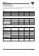
Absolute Maximum Ratings
T
amb
= 25 °C, unless otherwise specified
Stresses in excess of the absolute Maximum Ratings can cause permanent damage to the device. Functional operation of the device is
not implied at these or any other conditions in excess of those given in the operational sections of this document. Exposure to absolute
Maximum Rating for extended periods of the time can adversely affect reliability.
Input
Output
Coupler
Parameter Test condition Symbol Value Unit
Reverse voltage V
R
6.0 V
Forward current I
F
60 mA
Surge current t ≤ 10 µs I
FSM
2.5 A
Power dissipation P
diss
100 mW
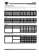
Parameter Test condition Symbol Value Unit
Collector-emitter breakdown
voltage
BV
CEO
70 V
Emitter-base breakdown
voltage
BV
EBO
7.0 V
Collector current I
C
50 mA
t < 1.0 ms I
C
100 mA
Power dissipation P
diss
150 mW
Parameter Test condition Symbol Value Unit
Isolation test voltage (between
emitter & detector referred to
climate DIN 50014,
part 2, Nov. 74)
t = 1 sec V
ISO
5300 V
RMS
Creepage distance ≥ 7.0 mm
Clearance distance ≥ 7.0 mm
Isolation thickness between
emitter and detector
≥ 0.4 mm
Comparative tracking index per
DIN IEC 112/VDE0303, part 1
175
Isolation resistance V
IO
= 500 V, T
amb
= 25 °C R
IO
≥ 10
12
Ω
V
IO
= 500 V, T
amb
= 100 °C R
IO
≥1 0
11
Ω
Storage temperature T
stg
- 55 to + 150 °C
Operating temperature T
amb
- 55 to + 100 °C
Soldering temperature max. 10 s, dip soldering:
distance to seating plane
≥ 1.5 mm
T
sld
260 °C