
Datasheet


BYG20D, BYG20G, BYG20J
www.vishay.com
Vishay General Semiconductor
Revision: 19-Feb-15
4
Document Number: 88958
For technical questions within your region: DiodesAmericas@vishay.com
, DiodesAsia@vishay.com, DiodesEurope@vishay.com
THIS DOCUMENT IS SUBJECT TO CHANGE WITHOUT NOTICE. THE PRODUCTS DESCRIBED HEREIN AND THIS DOCUMENT
ARE SUBJECT TO SPECIFIC DISCLAIMERS, SET FORTH AT www.vishay.com/doc?91000
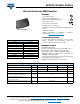
Fig. 7 - Reverse Recovery Charge vs. Forward Current Fig. 8 - Thermal Response
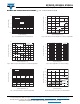
PACKAGE OUTLINE DIMENSIONS in inches (millimeters)
0
50
100
150
200
0 0.2 0.4 0.6 0.8
1.0
Reverse Recovery Charge (nC)
Forward Current (A)
I
R
= 0.5 A, i
R
= 0.125 A
T
A
= 125 °C
T
A
= 100 °C
T
A
= 75 °C
T
A
= 25 °C
T
A
= 50 °C
1
10
100
1000
Thermal Resistance for Pulse Cond. (K/W)
Pulse Length (s)
10
-5
10
-4
10
-3
10
-2
10
-1
10
0
10
1
10
2
Single Pulse
125 K/W DC
t
p
/T = 0.5
t
p
/T = 0.2
t
p
/T = 0.1
t
p
/T = 0.02
t
p
/T = 0.05
t
p
/T = 0.01
0.008 (0.203)
0.194 (4.93)
0.208 (5.28)
0.157 (3.99)
0.177 (4.50)
0.100 (2.54)
0.110 (2.79)
0.078 (1.98)
0.090 (2.29)
0.006 (0.152)
0.012 (0.305)
0.049 (1.25)
0.065 (1.65)
Cathode Band
0 (0)
DO-214AC (SMA)
Mounting Pad Layout
0.074 (1.88)
MAX.
0.208 (5.28)
REF.
0.066 (1.68)
MIN.
0.060 (1.52)
MIN.
0.030 (0.76)
0.060 (1.52)