
Datasheet

Document Number: 88838 For technical questions within your region, please contact one of the following: www.vishay.com
Revision: 04-Nov-09 DiodesAmericas@vishay.com
, DiodesAsia@vishay.com, DiodesEurope@vishay.com 1
General Purpose Plastic Rectifier
BY251P thru BY255P
Vishay General Semiconductor
FEATURES
• Low forward voltage drop
• Low leakage current, I
R
less than 0.1 μA
• High forward surge capability
• Solder dip 275 °C max. 10 s, per JESD 22-B106
• Compliant to RoHS directive 2002/95/EC and in
accordance to WEEE 2002/96/EC
TYPICAL APPLICATIONS
For use in general purpose rectification of power supplies,
inverters, converters and freewheeling diodes application.
Note
• These devices are not AEC-Q101 qualified.
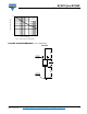
MECHANICAL DATA
Case: DO-201AD, molded epoxy body
Molding compound meets UL 94 V-0 flammability rating
Base P/N-E3 - RoHS compliant, commercial grade
Terminals: Matte tin plated leads, solderable per
J-STD-002 and JESD 22-B102
E3 suffix meets JESD 201 class 1A whisker test
Polarity: Color band denotes cathode end
PRIMARY CHARACTERISTICS
I
F(AV)
3.0 A
V
RRM
200 V to 1300 V
I
FSM
150 A
I
R
5.0 μA
V
F
1.1 V
T
J
max. 150 °C
DO-201AD
MAXIMUM RATINGS (T
A
= 25 °C unless otherwise noted)
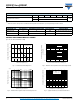
PARAMETER SYMBOL BY251P BY252P BY253P BY254P BY255P UNIT
Maximum repetitive peak reverse voltage V
RRM
200 400 600 800 1300 V
Maximum RMS voltage V
RMS
140 280 420 560 910 V
Maximum DC blocking voltage V
DC
200 400 600 800 1300 V
Maximum average forward rectified current
10 mm lead length
I
F(AV)
3.0 A
Peak forward surge current 10 ms single half
sine-wave superimposed on rated load
I
FSM
150 A
Maximum full load reverse current, full cycle average
10 mm lead length
I
R(AV)
100 μA
Operating junction and storage temperature range T
J
, T
STG
- 55 to + 150 °C
ELECTRICAL CHARACTERISTICS (T
A
= 25 °C unless otherwise noted)
PARAMETER TEST CONDITIONS SYMBOL BY251P BY252P BY253P BY254P BY255P UNIT
Maximum instantaneous
forward voltage
3.0 A V
F
1.1 V
Maximum reverse current
at rated DC blocking voltage
T
A
= 25 °C I
R
5.0 μA
Maximum reverse
recovery time
I
F
= 0.5 A, I
R
= 1.0 V,
I
rr
= 0.25 A
t
rr
3.0 μs
Typical junction capacitance 4.0 V, 1 MHz C
J
40 pF