
Datasheet

Document Number: 88526 For technical questions within your region, please contact one of the following: www.vishay.com
Revision: 20-Oct-09 DiodesAmericas@vishay.com
, DiodesAsia@vishay.com, DiodesEurope@vishay.com 1
Schottky Barrier Rectifier
1N5820 thru 1N5822
Vishay General Semiconductor
FEATURES
• Guardring for overvoltage protection
• Very small conduction losses
• Extremely fast switching
• Low forward voltage drop
• High forward surge capability
• High frequency operation
• Solder dip 275 °C max. 10 s, per JESD 22-B106
• Compliant to RoHS directive 2002/95/EC and in
accordance to WEEE 2002/96/EC
TYPICAL APPLICATIONS
For use in low voltage high frequency inverters,
freewheeling, dc-to-dc converters, and polarity protection
applications.
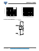
MECHANICAL DATA
Case: DO-201AD
Molding compound meets UL 94 V-0 flammability rating
Base P/N-E3 - RoHS compliant, commercial grade
Terminals: Matte tin plated leads, solderable per
J-STD-002 and JESD 22-B102
E3 suffix meets JESD 201 class 1A whisker test
Polarity: Color band denotes the cathode end
Note
(1)
Pulse test: 300 μs pulse width, 1 % duty cycle
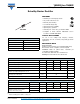
PRIMARY CHARACTERISTICS
I
F(AV)
3.0 A
V
RRM
20 V, 30 V, 40 V
I
FSM
80 A
V
F
0.475 V, 0.500 V, 0.525 V
T
J
max. 125 °C
DO-201AD
MAXIMUM RATINGS (T
A
= 25 °C unless otherwise noted)
PARAMETER SYMBOL 1N5820 1N5821 1N5822 UNIT
Maximum repetitive peak reverse voltage V
RRM
20 30 40 V
Maximum RMS voltage V
RMS
14 21 28 V
Maximum DC blocking voltage V
DC
20 30 40 V
Non-repetitive peak reverse voltage V
RSM
24 36 48 V
Maximum average forward rectified current
at 0.375" (9.5 mm) lead length at T
L
= 95 °C
I
F(AV)
3.0 A
Peak forward surge current, 8.3 ms single half sine-wave
superimposed on rated load
I
FSM
80 A
Operating junction and storage temperature range T
J
, T
STG
- 65 to + 125 °C
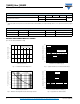
ELECTRICAL CHARACTERISTICS (T
A
= 25 °C unless otherwise noted)
PARAMETER TEST CONDITIONS SYMBOL 1N5820 1N5821 1N5822 UNIT
Maximum instantaneous forward voltage 3.0 V
F
(1)
0.475 0.500 0.525 V
Maximum instantaneous forward voltage 9.4 V
F
(1)
0.850 0.900 0.950 V
Maximum average reverse current
at rated DC blocking voltage
T
A
= 25 °C
I
R
(1)
2.0
mA
T
A
= 100 °C 20