
Datasheet

1N4933, 1N4934, 1N4935, 1N4936, 1N4937
www.vishay.com
Vishay General Semiconductor
Revision: 24-Jul-13
1
Document Number: 88508
For technical questions within your region: DiodesAmericas@vishay.com
, DiodesAsia@vishay.com, DiodesEurope@vishay.com
THIS DOCUMENT IS SUBJECT TO CHANGE WITHOUT NOTICE. THE PRODUCTS DESCRIBED HEREIN AND THIS DOCUMENT
ARE SUBJECT TO SPECIFIC DISCLAIMERS, SET FORTH AT www.vishay.com/doc?91000
Fast Switching Plastic Rectifier
FEATURES
• Fast switching for high efficiency
• Low forward voltage drop
• Low leakage current
• High forward surge capability
• Solder dip 275 °C max. 10 s, per JESD 22-B106
• Material categorization: For definitions of compliance
please see www.vishay.com/doc?99912
TYPICAL APPLICATIONS
For use in fast switching rectification of power supply,
inverters, converters and freewheeling diodes for consumer
and telecommunication.
Note
• These devices are not AEC-Q101 qualified.
MECHANICAL DATA
Case: DO-204AL, molded epoxy body
Molding compound meets UL 94 V-0 flammability rating
Base P/N-E3 - RoHS-compliant, commercial grade
Terminals: Matte tin plated leads, solderable per
J-STD-002 and JESD 22-B102
E3 suffix meets JESD 201 class 1A whisker test
Polarity: Color band denotes cathode end
PRIMARY CHARACTERISTICS
I
F(AV)
1.0 A
V
RRM
50 V, 100 V, 200 V, 400 V, 600 V
I
FSM
30 A
t
rr
200 ns
I
R
5.0 μA
V
F
1.2 V
T
J
max. 150 °C
Package DO-204AL (DO-41)
Diode variation Single die
DO-204AL (DO-41)
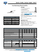
MAXIMUM RATINGS (T
A
= 25 °C unless otherwise noted)
PARAMETER SYMBOL 1N4933 1N4934 1N4935 1N4936 1N4937 UNIT
Maximum repetitive peak reverse voltage V
RRM
50 100 200 400 600 V
Maximum RMS voltage V
RMS
35 70 145 280 420 V
Maximum DC blocking voltage V
DC
50 100 200 400 600 V
Maximum average forward rectified current
0.375" (9.5 mm) lead length at T
A
= 75 °C
I
F(AV)
1.0 A
Peak forward surge current 8.3 ms single half sine-wave
superimposed on rated load
I
FSM
30 A
Maximum reverse recovery current I
RM
2.0 A
Operating junction and storage temperature range T
J
, T
STG
- 50 to + 150 °C
ELECTRICAL CHARACTERISTICS (T
A
= 25 °C unless otherwise noted)
PARAMETER TEST CONDITIONS SYMBOL 1N4933 1N4934 1N4935 1N4936 1N4937 UNIT
Maximum instantaneous
forward voltage
1.0 A V
F
1.2 V
Maximum DC reverse current
at rated DC blocking voltage
T
A
= 25 °C
I
R
5.0
μA
T
A
= 100 °C 100
Maximum reverse recovery time
I
F
= 1.0 A, V
R
= 30 V,
dI/dt = 50 A/μs, I
rr
= 10 % I
RM
t
rr
200 ns
Typical junction capacitance 4.0 V, 1 MHz C
J
12 pF