
Datasheet


1N4001GP, 1N4002GP, 1N4003GP, 1N4004GP, 1N4005GP, 1N4006GP, 1N4007GP
www.vishay.com
Vishay General Semiconductor
Revision: 04--Dec-13
1
Document Number: 88504
For technical questions within your region: DiodesAmericas@vishay.com
, DiodesAsia@vishay.com, DiodesEurope@vishay.com
THIS DOCUMENT IS SUBJECT TO CHANGE WITHOUT NOTICE. THE PRODUCTS DESCRIBED HEREIN AND THIS DOCUMENT
ARE SUBJECT TO SPECIFIC DISCLAIMERS, SET FORTH AT www.vishay.com/doc?91000
Glass Passivated Junction Plastic Rectifier
TYPICAL APPLICATIONS
For use in general purpose rectification of power supplies,
inverters, converters and freewheeling diodes for both
consumer, and automotive applications.
FEATURES
• Superectifier structure for high reliability
application
• Cavity-free glass-passivated junction
• Low forward voltage drop
• Low leakage current, typical I
R
less than 0.1 μA
• High forward surge capability
• Solder dip 275 °C max. 10 s, per JESD 22-B106
• AEC-Q101 qualified
• Material categorization: For definitions of compliance
please see www.vishay.com/doc?99912
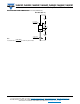
MECHANICAL DATA
Case: DO-204AL (DO-41), molded epoxy over glass body
Molding compound meets UL 94 V-0 flammability rating
Base P/N-E3 - RoHS-compliant, commercial grade
Base P/NHE3 - RoHS-compliant, AEC-Q101 qualified
Terminals: Matte tin plated leads, solderable per
J-STD-002 and JESD 22-B102
E3 suffix meets JESD 201 class 1A whisker test, HE3 suffix
meets JESD 201 class 2 whisker test
Polarity: Color band denotes cathode end
Note
• For part numbers with “E” suffix, they are”-E3” commercial
grade only
Notes
(1)
JEDEC
®
registered values
(2)
For device using on bridge rectifier application
PRIMARY CHARACTERISTICS
I
F(AV)
1.0 A
V
RRM
50 V, 100 V, 200 V, 400 V, 600 V,
800 V, 1000 V
I
FSM
(8.3 ms sine-wave) 30 A
I
FSM
(square wave t
p
= 1 ms) 45 A
I
R
5.0 μA
V
F
1.1 V
T
J
max. 175 °C
Package DO-204AL (DO-41)
Diode variations Single die
DO-204AL (DO-41)
SUPERECTIFIER
®
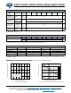
MAXIMUM RATINGS (T
A
= 25 °C unless otherwise noted)
PARAMETER SYMBOL
1N4001GP 1N4002GP 1N4003GP 1N4004GP 1N4005GP 1N4006GP 1N4007GP
UNIT
Maximum repetitive peak
reverse voltage
V
RRM
50 100 200 400 600 800 1000 V
Maximum RMS voltage V
RMS
(1)
35 70 140 280 420 560 700 V
Maximum DC blocking voltage V
DC
(1)
50 100 200 400 600 800 1000 V
Maximum average forward rectified
current 0.375" (9.5 mm) lead length
at T
A
= 75 °C
I
F(AV)
(1)
1.0 A
Peak forward surge current 8.3 ms
single half sine-wave
superimposed on rated load
I
FSM
(1)
30 A
Non-repetitive peak
forward surge current
square waveform
T
A
= 25 °C (fig. 3)
t
p
= 1 ms
I
FSM
(1)
45
A
t
p
= 2 ms 35
t
p
= 5 ms 30
Maximum full load reverse current,
full cycle average 0.375" (9.5 mm)
lead length T
A
= 75 °C
I
R(AV)
(1)
30 μA
Rating for fusing (t < 8.3 ms) I
2
t
(2)
3.7 A
2
s
Operating junction and
storage temperature range
T
J
, T
STG
(1)
- 65 to + 175 °C