
Owner's Manual

IRF840
www.vishay.com
Vishay Siliconix
S21-0883-Rev. E, 30-Aug-2021
1
Document Number: 91070
For technical questions, contact:
hvm@vishay.com
THIS DOCUMENT IS SUBJECT TO CHANGE WITHOUT NOTICE. THE PRODUCTS DESCRIBED HEREIN AND THIS DOCUMENT
ARE SUBJECT TO SPECIFIC DISCLAIMERS, SET FORTH AT
www.vishay.com/doc?91000
Power MOSFET
FEATURES
• Dynamic dV/dt rating
• Repetitive avalanche rated
• Fast switching
• Ease of paralleling
• Simple drive requirements
• Material categorization: for definitions of compliance
please see
www.vishay.com/doc?99912
Note
*
This datasheet provides information about parts that are
RoHS-compliant and / or parts that are non RoHS-compliant. For
example, parts with lead (Pb) terminations are not RoHS-compliant.
Please see the information / tables in this datasheet for details
DESCRIPTION
Third generation power MOSFETs from Vishay provide the
designer with the best combination of fast switching,
ruggedized device design, low on-resistance and
cost-effectiveness.
The TO-220AB package is universally preferred for all
commercial-industrial applications at power dissipation
levels to approximately 50 W. The low thermal resistance
and low package cost of the TO-220AB contribute to its
wide acceptance throughout the industry.
Notes
a. Repetitive rating; pulse width limited by maximum junction temperature (see fig. 11)
b. V
DD
= 50 V, starting T
J
= 25 °C, L = 14 mH, R
g
= 25 Ω, I
AS
= 8.0 A (see fig. 12)
c. I
SD
≤ 8.0 A, dI/dt ≤ 100 A/μs, V
DD
≤ V
DS
, T
J
≤ 150 °C
d. 1.6 mm from case
PRODUCT SUMMARY
V
DS
(V) 500
R
DS(on)
(Ω)V
GS
= 10 V 0.85
Q
g
max. (nC) 63
Q
gs
(nC) 9.3
Q
gd
(nC) 32
Configuration Single
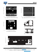
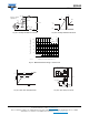
N-Channel MOSFET
G
D
S
TO-220AB
G
D
S
Available
Available
ORDERING INFORMATION
Package TO-220AB
Lead (Pb)-free IRF840PbF
Lead (Pb)-free and halogen-free IRF840PbF-BE3
ABSOLUTE MAXIMUM RATINGS (T
C
= 25 °C, unless otherwise noted)
PARAMETER SYMBOL LIMIT UNIT
Drain-source voltage V
DS
500 V
Gate-source voltage V
GS
± 20 V
Continuous drain current V
GS
at 10 V
T
C
= 25 °C
I
D
8.0
AT
C
= 100 °C 5.1
Pulsed drain current
a
I
DM
32
Linear derating factor 1.0 W/°C
Single pulse avalanche energy
b
E
AS
510 mJ
Repetitive avalanche current
a
I
AR
8.0 A
Repetitive avalanche energy
a
E
AR
13 mJ
Maximum power dissipation T
C
= 25 °C P
D
125 W
Peak diode recovery dV/dt
c
dV/dt 3.5 V/ns
Operating junction and storage temperature range T
J
, T
stg
-55 to +150
°C
Soldering recommendations (peak temperature)
d
For 10 s 300
Mounting torque 6-32 or M3 screw
10 lbf · in
1.1 N · m