SATA 6Gb/s Industrial mSATA Manual mSATA (mini-SATA, MO-300) is a non-volatile, solid-state storage device delivering Serial ATA performance, reliability and ruggedness for industrial and environmentally challenging applications. Manual PSFEM2xxxGRxxx Revision A10 www.vikingtechnology.
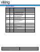
Revision History Date 4/10/13 5/10/13 6/26/13 7/11/13 Revision X1 A A1 A2 7/24/13 A3 8/12/13 A4 8/14/13 A5 9/09/13 A6 10/22/13 A7 1/15/14 A8 5/15/14 A9 7/24/14 A10 Manual PSFEM2xxxGRxxx Revision A10 www.vikingtechnology.com Description Preliminary release Initial Release Fix PN’s Add Power Consumption Revise SMART table. Added AES info. Add product image to 1st page. Create separate datasheets for 6Gbps. Revise extended SMART attributes. Changed Client to Industrial. Added SLC PN’s Add 3.
Legal Information Legal Information Copyright© 2014 Sanmina Corporation. All rights reserved. The information in this document is proprietary and confidential to Sanmina Corporation. No part of this document may be reproduced in any form or by any means or used to make any derivative work (such as translation, transformation, or adaptation) without written permission from Sanmina.
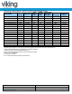
Ordering Information: mSATA SSD Solid-State Drive Part Numbers VRFEM2030GRIWMxx VRFEM2060GRIYMxx VRFEM2120GRITMxx VRFEM2030GRCWMxx VRFEM2060GRCYMxx VRFEM2120GRCTMxx VRFEM2240GRCVMxx VRFEM2030GRCWExx VRFEM2030GRCYExx VRFEM2060GRCYExx VRFEM2120GRCTExx VRFEM2240GRCVExx VRFEM2030GRCWSxx VRFEM2060GRCYSxx VRFEM2120GRCTSxx VRFEM2030GRIWSxx VRFEM2060GRIYSxx VRFEM2120GRITSxx SATA Interface Application 6Gbps 6Gbps 6Gbps 6Gbps 6Gbps 6Gbps 6Gbps 6Gbps 6Gbps 6Gbps 6Gbps 6Gbps 6Gbps 6Gbps 6Gbps 6Gbps 6Gbps 6Gbps Indu
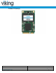
Product Picture(s) mSATA Top View Manual PSFEM2xxxGRxxx Revision A10 www.vikingtechnology.
Industrial SSD’s – Viking’s Industrial SSD contains sophisticated provisions to protect firmware and data from corruption due to unexpected power loss. However, an Industrial SSD by industry definition does not contain on-board capacitance. Should power fail unexpectedly, “in-flight” write data may be lost. Industrial SSD’s are best used in designs that manage power fail events at the system level. Manual PSFEM2xxxGRxxx Revision A10 www.vikingtechnology.
Table of Contents 1 INTRODUCTION 10 1.1 Features 10 1.2 Block Diagram 11 1.3 SATA Interface 12 2 2.1 PRODUCT SPECIFICATIONS Performance 13 13 2.2 Timing 2.2.1 STANDBY IMMEDIATE Command 13 13 2.3 Electrical Characteristics 2.3.1 Absolute Maximum Ratings 2.3.2 Supply Voltage 2.3.3 Supply Current 2.3.4 Power Consumption 14 14 14 15 15 2.4 Environmental Conditions 2.4.1 Temperature and Altitude 2.4.2 Shock and Vibration 2.4.3 Electromagnetic Immunity 15 15 16 16 2.5 16 Reliability 2.
5.1 ATA Commands 5.1.1 48-Bit Address Command Set 5.1.2 ATA General Feature Command Set 5.1.3 Device Configuration Overlay Command Set 5.1.4 General Purpose Log Command Set 5.1.5 Host Protected Area Command Set 5.1.6 Power Management Command Set 5.1.7 Security Mode Feature Set 5.1.8 Identify Device Data 5.1.1 S.M.A.R.T. Support 5.1.2 SATA 3.0 S.M.A.R.T. Command Set 31 32 32 32 32 33 33 33 34 37 38 5.2 SATA Commands 5.2.
Table of Tables Table 2-1: Maximum Sustained Read and Write Bandwidth ____________________________ 13 Table 2-2: Random Read and Write Input/Output Operations per Second (IOPS) ___________ 13 Table 2-3: Timing Specifications _________________________________________________ 13 Table 2-4: STANDBY IMMEDIATE Timing _________________________________________ 14 Table 2-5: Absolute Maximum Ratings ____________________________________________ 14 Table 2-6: Operating Voltage ________________________________________
1 Introduction Viking’s rugged industrial designed SSD’s offer the highest flash storage reliability and performance in harsh environments such as shock, vibration, humidity, altitude, ESD, and extreme temperatures. 1.1 Features The SSD delivers the following features: • Offers seamless SATA Revision 3.0 interface support for SATA up to 6Gb/s • Low overall SSD power consumption • Supports Native Command Queuing (NCQ) to 32 commands • Compatible with all major SLC, MLC and eMLC flash technologies • S.M.A.R.
1.2 Block Diagram Figure 1-1: High-Level Block Diagram Notes: 5V not supported on VRFEM2xxxGRxxxJx PN’s Manual PSFEM2xxxGRxxx Revision A10 www.vikingtechnology.
1.3 SATA Interface • • • The Serial ATA (SATA) interface is compliant with the SATA IO Serial ATA specification, revision 3.0 that supports SATA up to 6Gb/s. The SATA interface connects the host computer to the SSD subsystem. The SATA interface runs at a maximum speed of 6 Gbps (Giga-bits per second). If the host computer is unable to negotiate a speed of 6 Gbps, the SATA interface automatically renegotiates to a speed of 3 Gbps or 1.5 Gbps.
2 Product Specifications 2.1 Performance Table 2-1: Maximum Sustained Read and Write Bandwidth Access Type Sequential Read, 256K Sequential Write, 256K VRFEM2xxxGRxxx Up to 508 MB/s Up to 364 MB/s Notes: 1. Performance measured using IOmeter 06 with queue depth set to 32. 2. Write Cache enabled with DDR cache. 3. Refer to Application Note AN0006 for Viking SSD Benchmarking Methodology. 4.
the use of the hold-up circuit. Note that SMART attribute 174 "Unexpected Power Loss" records the number of non-graceful power cycle events. Table 2-4: STANDBY IMMEDIATE Timing Power Cycle Endurance STANDBY IMMEDIATE to WE completed Min - Max 72.9 Unit ms Notes: From Standby Immediate command to NAND Write Protect enable. 2.3 Electrical Characteristics 2.3.1 Absolute Maximum Ratings Values shown are stress ratings only. Functional operation outside normal operating values is not implied.
2.3.3 Supply Current Table 2-7: Current Draw Voltage 3.3V 5.0V Typical1 850 / 600 80 14 tbd tbd tbd Mode Read/Writes (Average RMS) Idle Slumber Read/Writes (Average RMS) Idle Slumber Unit mA mA mA mA mA mA Notes: 1. Measured using 60GB MLC, VRFEM2060GRCYMTJ 2. 5V not supported on VRFEM2xxxGRxxxJx PN’s 2.3.4 Power Consumption All onboard power requirements of the SSD are derived from the SATA 3.3V or 5.0V input rail.
2.4.2 Shock and Vibration SSD products are tested in accordance with environmental specification for shock and vibration Table 2-10: Shock and Vibration Specifications Stimulus Description 50g, 11ms, 3 shocks applied in each direction on 3 mutually perpendicular axes X, Y, Z 16.4g rms 10-2,000 Hz, 3 axes Shock Vibration 2.4.3 Electromagnetic Immunity mSATA is an embedded product for host systems and is designed not to impair with system functionality or hinder system EMI/FCC compliance. 2.
2.6.1 Quick Erase Quick Erase has been designed to remove data under prompt and urgent situation and is triggered by sending an ATA Command. Input Info of Executing Quick Erase Command Normal Output Info of Executing Quick Erase Command Device/Head Register: DEV shall indicate the selected device. Status Register: BSY shall be cleared to zero indicating command completion. DRDY shall be set to one. DF (Device Fault) shall be cleared to zero. DRQ shall be cleared to zero. ERR shall be cleared to zero. 2.
different patterns to sanitize the flash media. Some of the more common military or government purge routines are defined in the following table and the data security features of the drive comply with Department of Defense (DoD) and US military data security standards. Table 2-12: Military Secure Erase / Sanitize Routines Standard Action SSD Code1 Note 1 NSA/CSS 9-12 Erase and overwrite all locations with a known unclassified pattern.
2.6.2.1 AFSSI 5020 Pattern: 1) To erase the whole disk. 2) To fill the whole disk with random data. Input Info of Executing AFSSI 5020 Command Normal Output Info of Executing AFSSI 5020 Command Device/Head Register: DEV shall indicate the selected device. Status Register: BSY shall be cleared to zero indicating command completion. DRDY shall be set to one. DF (Device Fault) shall be cleared to zero. DRQ shall be cleared to zero. ERR shall be cleared to zero. Manual PSFEM2xxxGRxxx Revision A10 www.
2.6.2.2 DOD 5220.22-M Pattern: 1) To fill the whole disk with fixed character pattern of 0x55. 2) To erase the whole disk. Input Info of Executing DoD 5220.22-M Command Normal Output Info of Executing DoD 5220.22-M Command Device/Head Register: DEV shall indicate the selected device. Status Register: BSY shall be cleared to zero indicating command completion. DRDY shall be set to one. DF (Device Fault) shall be cleared to zero. DRQ shall be cleared to zero. ERR shall be cleared to zero.
2.6.2.3 USA NAVY NAVSO P-5239-26 Pattern: 1) To erase the whole disk. 2) To fill the whole disk with random data. 3) To erase the whole disk again. Input Info of Executing USA Navy NAVSO P-5239-26 Command Normal Output Info of Executing USA Navy NAVSO P-5239-26 Command Device/Head Register: DEV shall indicate the selected device. Status Register: BSY shall be cleared to zero indicating command completion. DRDY shall be set to one. DF (Device Fault) shall be cleared to zero. DRQ shall be cleared to zero.
2.6.2.4 NSAMANUAL 130-2 Pattern: 1) To erase the whole disk. 2) To fill the whole disk with random data. 3) To fill the whole disk with random data one more time. 4) To erase the whole disk again. 5) To fill the whole disk with fixed character pattern of 0x55. Input Info of Executing NSA Manual 130-2 Command Normal Output Info of Executing NSA Manual 130-2 Command Device/Head Register: DEV shall indicate the selected device. Status Register: BSY shall be cleared to zero indicating command completion.
2.6.2.5 USA-ARMY 380-19 Pattern: 1) To erase the whole disk. 2) To fill the whole disk with random data. 3) To fill the whole disk with fixed character pattern of 0x55. 4) To fill the whole disk with fixed character pattern of 0xAA. Input Info of Executing USA-Army 380-19 Command Normal Output Info of Executing USA-Army 380-19 Command Device/Head Register: DEV shall indicate the selected device. Status Register: BSY shall be cleared to zero indicating command completion. DRDY shall be set to one.
2.6.2.6 NISPOMSUP CHAP 8, SECT. 8-501 Pattern: 1) To fill the whole disk with fixed character pattern of 0x55. 2) To fill the whole disk with fixed character pattern of 0xAA. 3) To fill the whole disk with random data. Input Info of Executing NISPOMSUP chap 8, Sect. 8-501 Command Normal Output Info of Executing NISPOMSUP chap 8, Sect. 8-501 Command Device/Head Register: DEV shall indicate the selected device. Status Register: BSY shall be cleared to zero indicating command completion.
2.6.2.7 NSA/CSS 9-12 Pattern: 1) To fill the whole disk with fixed character pattern of 0x55. Input Info of Executing NSA/CSS 9-12 Command Normal Output Info of Executing NSA/CSS 9-12 Command Device/Head Register: DEV shall indicate the selected device. Status Register: BSY shall be cleared to zero indicating command completion. DRDY shall be set to one. DF (Device Fault) shall be cleared to zero. DRQ shall be cleared to zero. ERR shall be cleared to zero. Manual PSFEM2xxxGRxxx Revision A10 www.
2.6.2.8 AFSSI 8580 Pattern: 1) To fill the whole disk with fixed character pattern of 0x55. 2) To fill the whole disk with fixed character pattern of 0xAA. 3) To fill the whole disk with random data. Input Info of Executing AFSSI 8580 Command Normal Output Info of Executing AFSSI 8580 Command Device/Head Register: DEV shall indicate the selected device. Status Register: BSY shall be cleared to zero indicating command completion. DRDY shall be set to one. DF (Device Fault) shall be cleared to zero.
mSATA (MO-300) Form Factor Min Max Height (mm) Width (mm) Length (mm) 4.85 29.70 30.00 50.65 50.95 Figure 3-1: Dimensions Manual PSFEM2xxxGRxxx Revision A10 www.vikingtechnology.
Notes: All dimensions are in millimeters Manual PSFEM2xxxGRxxx Revision A10 www.vikingtechnology.
3.1 mSATA SSD Weight The weight of the mSATA (mini-SATA, MO-300) SSD is approximately 8 grams. 4 Pin and Signal Descriptions 4.1 Signal and Power Description Tables Table 4-1: Mini PCIe Connector Pin Signal Definitions Pin # Type Description P1 Reserved No Connect P2 +3.3V or 5.0V 3.3V or 5.
Pin # Type Description P29 GND Return Current Path P30 NC No Connect P31 -A Host Transmitter Differential Signal Pair P32 NC No Connect P33 +A Host Transmitter Differential Signal Pair P34 GND Return Current Path P35 GND Return Current Path P36 Reserved No Connect P37 GND Return Current Path P38 Reserved No Connect P39 +3.3V or 5.0V 3.3V or 5.0V Source P40 GND Return Current Path P41 +3.3V or 5.0V 3.3V or 5.
5.
5.1.1 48-Bit Address Command Set SSD supports the 48-Bit Address command set consisting of: • Flush Cache Ext • Read DMA Ext • Read native Max Address Ext • Read Sector(s) Ext • Set Max Address Ext • Write DMA Ext • Write Multiple Ext • Write Sector(s) Ext 5.1.
5.1.5 Host Protected Area Command Set SSD supports the Host Protected Area command set consisting of: • Read Native Max Address • Read Native Max Address Ext • Set Max Address • Set Max Address Ext • Set Max Freeze Lock (optional) • Set Max Lock (optional) • Set Max Set Password (optional) • Set Max Unlock (optional) 5.1.
5.1.8 Identify Device Data The table below lists the sector data that will be returned by the SSD upon an IDENTIFY DEVICE command.
F: Fixed V: Variable X: Both Default Value 67 F 0078h 68 F 0078h 69 F 0100h 70 F 71-74 F 75 76 77 78 79 80 81 82 83 84 85 86 87 88 F F F F V F F F F F V V V V 0000h 000000000000000 0h 001Fh 0706h 0000h 0044h 0040H 01F8h 0000h 346Bh 70D9h 6023h 3469h BC01h 6023h 003Fh 89 F 001Eh 90 F 001Eh 91 92 V V 0000h FFFEh 93 F 0000h 94 V 0000h 95 96 97 98-99 F V V F 0000h 0000h 0000h 0000h 100-103 V 8GB-256GB 104 V 0000h 105 F 0000h 106 F 4000h 107 F 0000h Word Manual
Word F: Fixed V: Variable X: Both Default Value 108-111 F 112-115 F 116 117-118 119 120 121-126 V F F F F 000000000000000 0h 000000000000000 0h 0000h 00000000h 4015h 4015h 0h 127 F 0h 128 129-159 V X 0021h 0h 160 F 0h 161-167 X 168 F 0h Tbd 3h: 2.5 inch 4h: 1.8 inch 5h: < 1.
Word F: Fixed V: Variable X: Both 236-254 F 255 X Default Value 0h XXA5h XX is variable Description DOWNLOAD MICROCODE command for mode 03h Reserved Integrity word (Checksum and Signature) Table 5-3: Capacity specific Device Identification *1 *2 *3 *4 (Word 1/Word 54) (Word 57-58) (Word 60-61) (Word 100-103) 32 tbd tbd tbd tbd 64 tbd tbd tbd tbd 128 tbd tbd tbd tbd 256 tbd tbd tbd tbd 512 tbd tbd tbd tbd 1000 tbd tbd tbd tbd Capacity (GB) 5.1.1 S.M.A.R.T.
references for topics and details not addressed here. Further, it is recommended to consult the list of public S.M.A.R.T. attributes. See the AT Attachment standard for implementation details. 5.1.2 SATA 3.0 S.M.A.R.T. Command Set The supported S.M.A.R.T. command set is listed in the table below. See the AT Attachment standard for implementation details. Table 5-4: S.M.A.R.T. Command Set Value (hex) Command 00-CF Reserved D0 S.M.A.R.T. read attributes D1* S.M.A.R.T. read threshold D2 S.M.A.R.T.
SMART Attribute ID Description A8h SATA PHY Error Count (only record from power on, when power off this value will clear to zero) this value include all PHY error count, ex data FIS CRC ,code error, disparity error ,command FIS CRC …..
0 ID 09h 0Ch A8h AAh ADh B1h B5h B6h BBh C0h C2h C7h DAh E7h E8h E9h F1h F2h F3h F4h F5h F6h FAh FBh 1 2 Flag Flag 3 4 Value Worse 5 6 7 8 9 11 DATA 00h 64h 64h 0 0 0 00h 12h 00h 64h 64h Power on/off cycles 0 0 0 00h 12h 00h 64h 64h SATA PHY error count 0 0 0 00h 03h 00h Note 1 Note 1 Early bad block NO Later bad block NO 0 0Ah 12h 00h 64h 64h Max erase count (MAX 65535) 00 0 00h 00h 00h 00h 00h The value 0 0 0 00h 12h 00h 00h 00h Total pr
0 ID FCh 1 2 Flag Flag 02h 00h 3 4 5 6 7 Value Worse DATA 64h 64h CRC write Count 8 9 10 11 Threshold 0 00h Note 1 Formula: MABN: Maximum acceptable bad block number CBBN: Current bad block number Value = ((MABN – CBBN)/ (MABN )) x 100 This formula calculates percentage of spare blocks. Value will be from 100 to 1 Note 2: Average erase count / MAX erase count (SLC 100000, MLC 5000) * 100 (percentage) 5.1.2.2Off-line Mode SSD’s support the optional 28-bit S.M.A.R.T.
5.2.1 Native Command Queuing (NCQ) SSD’s support the Native Command Queuing (NCQ) command set, which consists of • READ FPDMA QUEUED • WRITE FPDMA QUEUED Note: With a maximum queue depth less than or equal to 32. 6 References • Serial ATA Specification, Revision 3 Manual PSFEM2xxxGRxxx Revision A10 www.vikingtechnology.
7 Glossary This document incorporates many industry and device-specific words. Use the following list to define a variety of terms and acronyms. Term Definition ATA ATAPI Advanced Technology Attachment Advanced Technology Attachment Packet Interface Bit error rate, or percentage of bits that have errors relative to the total number of bits received Device Initiated Link Power Management. The ability of the device to request SATA link power state changes.