
User`s manual


BIOS Setup
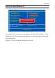
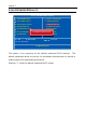
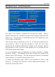
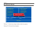
DRAM CLOCK/DRIVE CONTROL
: Move
F5: Previous Values F6: Fail-Safe Defaults F7: Optimized Defaults
Enter: Select +/-/PU/PD: Value F10: Save ESC: Exit F1: General Help
Menu Level
Item Help
DRAM Clock [By SPD]
DRAM Timing [Manual]
Bank Interleave
[Disabled]
Precharge to Active(Trp)
[4T]
Active to CMD(Trcd)
[4T]
PnP / PCI Configurations
Phoenix - AwardBIOS CMOS Setup Utility
REF to ACT/REF (Trfc)
[25T]
ACT(0) to ACT(1) (TRRD)
[3T]
Write to read CMD (Twtr)
Write Recovery Time (Twr)
[4T]
RDSAIT mode
[Auto]
SDRAM CAS Latency [DDR/DDR2]
[2.5 / 4]
Active to Precharge(Tras)
[07T]
Read to Precharge (Trtp)
[2T]
x RDSAIT selection
03
[1T/2T]
DRAM Clock
The chipset supports synchronous and asynchronous mode between host
clock and DRAM clock frequency.
Settings: [By SPD, 100 MHz, 133 MHz, 166 MHz, 200MHz, 266MHz, 333MHz]
DRAM Timing
The value in this field depends on the memory modules installed in your
system. Changing the value from the factory setting is not recommended
unless you install new memory that has a different performance rating than
the original modules.
Settings: [Manual, Auto By SPD]
SDRAM CAS Latency [DDR/DDR2]
Settings: [1.5/2, 2/3, 2.5/4, 3/5]
Bank Interleave
Settings: [Disabled, 2 Bank, 4 Bank, 8 Bank]
Precharge to Active (Trp)
Settings: [2T, 3T, 4T, 5T]