
Data Sheet


TB6560AHQ/AFG
2014-10-01
26
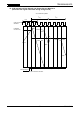
Test Points for AC Specifications
Figure 1 Timing Waveforms and Symbols
OSC-Charge DELAY:
The OSC waveform is converted into the internal OSC waveform by checking the level of a chopping wave.
The internal OSC signal is designed to be logic High when the OSC voltage is at 2 V or above, and to be logic
Low when the OSC voltage is at 0.5 V or below. However, there is a response delay and that there occurs a
peak-to-peak voltage variation.
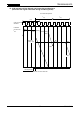
Figure 2 Timing Waveforms (OSC Signal)
CLK
t
CLK
t
CLK
t
pLH
t
pHL
VM
GND
t
r
t
f
10%
50%
90%
90%
50%
10%
OSC
Waveform
OSC Pin
Internal
Waveform
2 V
0.5 V