
Data Sheet


TB6560AHQ/AFG
2014-10-01
2
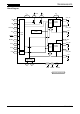
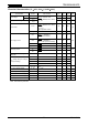
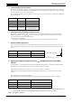
Block Diagram
M1
M2
CW/CCW
CLK
RESET
ENABLE
DCY1
DCY2
OSC
Input
circuit
OSC
V
DD
Maximum current
setting circuit
Thermal shutdown
circuit
Protect
M
O
Bridge
driver A
VM
A
OUT_AP
N
FA
VM
B
Bridge
driver B
OUT_BP
OUT_BM
N
FB
TQ1
TQ2
SGND
PGNDA
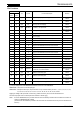
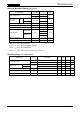
10/64
1/42
2/43
11/2, 4
9/61, 62
12/6, 7
8/55, 56
14/13, 14
13/10, 11
16/19, 20
18/25, 26
17/23
19/28
20/30, 31
23/36
22/35
21/33
3/45
5/48
4/47
25/39
24/38
7/53
15/16
6/50, 51
TB6560AHQ/TB6560AFG
PWM
control
circuit
PWM
control
circuit
OUT_AM
PGNDB