
Data Sheet


TB6560AHQ/AFG
2014-10-01
10
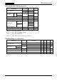
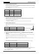
5. Torque Settings (Current Value)
The ratio of the current necessary for actual operations to the predefined current adjusted by an external
resistor can be selected as follows. The Weak Excitation mode should be selected to set a torque extremely
low like when the motor is at a fixed position.
Since the TQ2 and TQ1 pins have pull-down resistors, the 100 % torque setting is selected when TQ2 and
TQ1 are undriven.
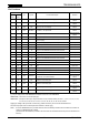
TQ2 TQ1 Current Ratio
L L 100 %
L H 75 %
H L 50 %
H H
20 %
(Weak excitation)
6. Calculation of the Predefined Output Current
To perform a constant current drive, the reference current should be adjusted by an external resistor.
Charging stops when the N
FA
(N
FB
) voltage reaches 0.5 V (when the torque setting is 100 %) so that a
current does not exceed the predefined level.
I
OUT
(A) = 0.5 (V) / R
NF
(Ω)
Example: To set the peak current to 1 A, the value of an external resistor should be 0.5 Ω.
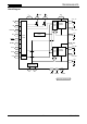
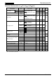
7. Protect and M
O
Output Pins
These are open-drain outputs. An external pull-up resistor should be added to these pins when in use.
If the TSD circuit is activated, Protect is driven Low. When the IC enters the Initial state, M
O
is driven
Low.
Pin State Protect M
O
Low Thermal shutdown Initial state
High-Z Normal operation Other than the initial state
Rest voltage of output terminal Mo and output terminal Protect reach 0.5 V (max) when I
O
is 1 mA.
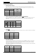
8. Adjusting the External Capacitor Value (C
OSC
) and Minimum Clock Pulse Width
(t
W(CLK)
)
A triangular-wave is generated internally by CR oscillation. The capacitor is externally connected to the
OSC pin. The recommended capacitor value is between 100 pF and 1000 pF.
Approximate equation: f
OSC
= 1/{ C
OSC
× 1.5 × (10/ C
OSC
+ 1)/66} × 1000 kHz
(Since this is an approximation formula, the calculation result may not be exactly equal to the actual
value.)
The approximate values are shown below.
The minimum clock pulse width (t
W(CLK)
) corresponds to the external capacitor (C
OSC
) as follows:
Capacitor Oscillating Frequency Minimum Clock Pulse Width t
W(CLK)
(Note 1)
1000 pF 44 kHz 90 µs (Note 2)
330 pF 130 kHz 30 µs
100 pF 400 kHz 10 µs (Note 2)
Note 1: When the frequency of an input clock signal is high, the C
OSC
value should be small so that the duty cycle
of an input clock pulse does not become extremely high (should be around 50 % or lower).
Note 2: Not tested in production.
Open-drain connection