
Data Sheet

Sensors
8 Freescale Semiconductor
MMA8452Q
2.3 I
2
C Interface Characteristic
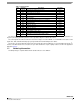
Table 4. I
2
C Slave Timing Values
(1)
1. All values referred to VIH (min) and VIL (max) levels.
Parameter Symbol
I
2
C Fast Mode
Unit
Min Max
SCL Clock Frequency
Pullup = 4.7 k
Ω, Cb = 20 pF
Pullup = 4.7 k
Ω, Cb = 40 pF
Pullup = 4.7 k
Ω, Cb = 400 pF
Pullup = 1 k
Ω, Cb = 20 pF
Pullup = 1 k
Ω, Cb = 400 pF
f
SCL
0
0
0
0
0
2.250
100
Nonfunctional
4.50
750
MHz
kHz
—
MHz
kHz
Bus Free Time between STOP and START Condition t
BUF
1.3 μs
Repeated START Hold Time t
HD;STA
0.6 μs
Repeated START Setup Time t
SU;STA
0.6 μs
STOP Condition Setup Time t
SU;STO
0.6 μs
SDA Data Hold Time
(2)
2. t
HD;DAT
is the data hold time that is measured from the falling edge of SCL, applies to data in transmission and the acknowledge.
t
HD;DAT
50
(3)
3. The maximum t
HD;DAT
could be 3.45 μs and 0.9 μs for Standard mode and Fast mode, but must be less than the maximum of t
VD;DAT
or t
VD;ACK
by a transition time.
μs
SDA Valid Time
(4)
4. t
VD;DAT
= time for Data signal from SCL LOW to SDA output (HIGH or LOW, depending on which one is worse).
t
VD;DAT
0.9
(3)
μs
SDA Valid Acknowledge Time
(5)
5. t
VD;ACK
= time for Acknowledgement signal from SCL LOW to SDA output (HIGH or LOW, depending on which one is worse).
t
VD;ACK
0.9
(3)
μs
SDA Setup Time t
SU;DAT
100
(6)
6. A Fast mode I
2
C device can be used in a Standard mode I
2
C system, but the requirement t
SU;DAT
250 ns must then be met. This will
automatically be the case if the device does not stretch the LOW period of the SCL signal. If such a device does stretch the LOW period of the
SCL signal, it must output the next data bit to the SDA line t
r
(max) + t
SU;DAT
= 1000 + 250 = 1250 ns (according to the Standard mode I
2
C
specification) before the SCL line is released. Also the acknowledge timing must meet this setup time
ns
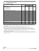
SCL Clock Low Time t
LOW
4.7 μs
SCL Clock High Time t
HIGH
4 μs
SDA and SCL Rise Time t
r
1000 ns
SDA and SCL Fall Time
(7) (8)
7. Cb = total capacitance of one bus line in pF.
8. The maximum t
f
for the SDA and SCL bus lines is specified at 300 ns. The maximum fall time for the SDA output stage t
f
is specified at 250 ns.
This allows series protection resistors to be connected in between the SDA and the SCL pins and the SDA/SCL bus lines without exceeding
the maximum specified t
f
.
t
f
300 ns
Pulse width of spikes on SDA and SCL that must be suppressed by input filter t
SP
50 ns