
Data Sheet
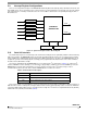

Sensors
Freescale Semiconductor 19
MMA8452Q
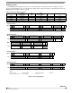
Note: Auto-increment addresses which are not a simple increment are highlighted in bold. The auto-increment addressing is only enabled when
device registers are read using I
2
C burst read mode. Therefore the internal storage of the auto-increment address is cleared whenever a
stop-bit is detected.
6.1 Data Registers
The following are the data registers for the MMA8452Q. For more information on data manipulation of the MMA8452Q, refer
to application note, AN4076.
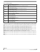
PULSE_THSZ
(1)(3)
R/W 0x25 0x26 00000000 0x00 Z pulse threshold
PULSE_TMLT
(1)(3)
R/W 0x26 0x27 00000000 0x00 Time limit for pulse
PULSE_LTCY
(1)(3)
R/W 0x27 0x28 00000000 0x00 Latency time for 2
nd
pulse
PULSE_WIND
(1)(3)
R/W 0x28 0x29 00000000 0x00 Window time for 2nd pulse
ASLP_COUNT
(1)(3)
R/W 0x29 0x2A 00000000 0x00 Counter setting for Auto-SLEEP
CTRL_REG1
(1)(3)
R/W 0x2A 0x2B 00000000 0x00 ODR = 800 Hz, STANDBY Mode.
CTRL_REG2
(1)(3)
R/W 0x2B 0x2C 00000000 0x00
Sleep Enable, OS Modes,
RST, ST
CTRL_REG3
(1)(3)
R/W 0x2C 0x2D 00000000 0x00 Wake from Sleep, IPOL, PP_OD
CTRL_REG4
(1)(3)
R/W 0x2D 0x2E 00000000 0x00 Interrupt enable register
CTRL_REG5
(1)(3)
R/W 0x2E 0x2F 00000000 0x00 Interrupt pin (INT1/INT2) map
OFF_X
(1)(3)
R/W 0x2F 0x30 00000000 0x00 X-axis offset adjust
OFF_Y
(1)(3)
R/W 0x30 0x31 00000000 0x00 Y-axis offset adjust
OFF_Z
(1)(3)
R/W 0x31 0x0D 00000000 0x00 Z-axis offset adjust
Reserved (do not modify) 0x40 – 7F — — — Reserved. Read return 0x00.
1. Register contents are preserved when transition from ACTIVE to STANDBY mode occurs.
2. Register contents are reset when transition from STANDBY to ACTIVE mode occurs.
3. Modification of this register’s contents can only occur when device is STANDBY mode except CTRL_REG1 ACTIVE bit and CTRL_REG2
RST bit.
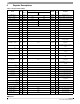
0x00 STATUS: Data Status Register (Read Only)
Bit 7 Bit 6 Bit 5 Bit 4 Bit 3 Bit 2 Bit 1 Bit 0
ZYXOW ZOW YOW XOW ZYXDR ZDR YDR XDR
Table 11. Register Address Map