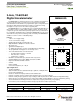
Document Number: MMA8452Q Rev 4.1, 08/2011 Freescale Semiconductor Data Sheet: Technical Data An Energy Efficient Solution by Freescale 3-Axis, 12-bit/8-bit MMA8452Q Digital Accelerometer The MMA8452Q is a smart low-power, three-axis, capacitive micromachined accelerometer with 12 bits of resolution. This accelerometer is packed with embedded functions with flexible user programmable options, configurable to two interrupt pins.
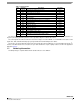
Contents 1 2 3 4 5 6 Block Diagram and Pin Description .................................................................................................................................. 3 1.1 Soldering Information .................................................................................................................................................. 5 Mechanical and Electrical Specifications .......................................................................................................
Application Notes for Reference The following is a list of Freescale Application Notes written for the MMA8451, 2, 3Q: • AN4068, Embedded Orientation Detection Using the MMA8451, 2, 3Q • AN4069, Offset Calibration of the MMA8451, 2, 3Q • AN4070, Motion and Freefall Detection Using the MMA8451, 2, 3Q • AN4071, High Pass Data and Functions Using the MMA8451, 2,3Q • AN4072, MMA8451, 2, 3Q Single/Double and Directional Tap Detection • AN4073, Using the 32 Sample First In First Out (FIFO) in the MMA8451Q • AN407
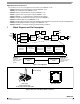
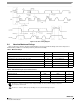
Figure 3 shows the device configuration in the 6 different orientation modes. These orientations are defined as the following: PU = Portrait Up, LR = Landscape Right, PD = Portrait Down, LL = Landscape Left, BACK and FRONT side views. There are several registers to configure the orientation detection and are described in detail in the register setting section.
Table 1. Pin Description Pin # Pin Name 1 VDDIO 2 BYP Description Pin Status Internal Power Supply (1.62 V - 3.6 V) Input Bypass capacitor (0.1 μF) Input 3 NC Leave open. Do not connect.
2 Mechanical and Electrical Specifications 2.1 Mechanical Characteristics Table 2. Mechanical Characteristics @ VDD = 2.5 V, VDDIO = 1.8 V, T = 25°C unless otherwise noted. Parameter Test Conditions Symbol Min FS[1:0] set to 00 2g Mode Measurement Range(1) Sensitivity FS[1:0] set to 01 4g Mode Typ FS ±4 ±8 FS[1:0] set to 00 2g Mode 1024 So g 512 FS[1:0] set to 10 8g Mode Sensitivity Accuracy(2) Unit ±2 FS[1:0] set to 10 8g Mode FS[1:0] set to 01 4g Mode Max counts/g 256 Soa ±2.
2.2 Electrical Characteristics Table 3. Electrical Characteristics @ VDD = 2.5 V, VDDIO = 1.8 V, T = 25°C unless otherwise noted. Parameter Test Conditions Supply Voltage Interface Supply Voltage Low Power Mode Symbol Min Typ Max Unit VDD(1) 1.95 2.5 3.6 V VDDIO(1) 1.62 1.8 3.6 V ODR = 1.56 Hz 6 ODR = 6.25 Hz 6 ODR = 12.5 Hz 6 ODR = 50 Hz 14 ODR = 100 Hz IddLP ODR = 200 Hz Normal Mode 44 ODR = 400 Hz 85 ODR = 800 Hz 165 ODR = 1.56 Hz 24 ODR = 6.25 Hz 24 ODR = 12.
2.3 I2C Interface Characteristic Table 4. I2C Slave Timing Values(1) Parameter Symbol I2C Fast Mode Min Max 0 0 0 0 0 2.250 100 Nonfunctional 4.50 750 Unit SCL Clock Frequency Pullup = 4.7 kΩ, Cb = 20 pF Pullup = 4.7 kΩ, Cb = 40 pF Pullup = 4.7 kΩ, Cb = 400 pF Pullup = 1 kΩ, Cb = 20 pF Pullup = 1 kΩ, Cb = 400 pF fSCL Bus Free Time between STOP and START Condition tBUF 1.3 μs Repeated START Hold Time tHD;STA 0.6 μs Repeated START Setup Time tSU;STA 0.
Figure 5. I2C Slave Timing Diagram 2.4 Absolute Maximum Ratings Stresses above those listed as “absolute maximum ratings” may cause permanent damage to the device. Exposure to maximum rating conditions for extended periods may affect device reliability. Table 5. Maximum Ratings Rating Symbol Value Unit Maximum Acceleration (all axes, 100 μs) gmax 5,000 g Supply Voltage VDD -0.3 to + 3.6 V Vin -0.3 to VDDIO + 0.3 V Drop Test Ddrop 1.
3 Terminology 3.1 Sensitivity The sensitivity is represented in counts/g. In 2g mode the sensitivity is 1024 counts/g. In 4g mode the sensitivity is 512 counts/g and in 8g mode the sensitivity is 256 counts/g. 3.2 Zero-g Offset Zero-g Offset (TyOff) describes the deviation of an actual output signal from the ideal output signal if the sensor is stationary. A sensor stationary on a horizontal surface will measure 0g in X-axis and 0g in Y-axis whereas the Z-axis will measure 1g.
5 Functionality The MMA8452Q is a low-power, digital output 3-axis linear accelerometer with a I2C interface and embedded logic used to detect events and notify an external microprocessor over interrupt lines.
5.3 Low Power Modes vs. High Resolution Modes The MMA8452Q can be optimized for lower power modes or for higher resolution of the output data. High resolution is achieved by setting the LNOISE bit in Register 0x2A. This improves the resolution but be aware that the dynamic range is limited to 4g when this bit is set. This will affect all internal functions and reduce noise. Another method for improving the resolution of the data is by oversampling.
5.6 Transient Detection The MMA8452Q has a built-in high pass filter. Acceleration data goes through the high pass filter, eliminating the offset (DC) and low frequencies. The high pass filter cut-off frequency can be set by the user to four different frequencies which are dependent on the Output Data Rate (ODR). A higher cut-off frequency ensures the DC data or slower moving data will be filtered out, allowing only the higher frequencies to pass.
PORTRAIT 90° PORTRAIT 90° Landscape to Portrait Trip Angle = 60° Portrait to Landscape Trip Angle = 30° 0° Landscape Figure 8. Illustration of Landscape to Portrait Transition 0° Landscape Figure 9. Illustration of Portrait to Landscape Transition Figure 10 illustrates the Z-angle lockout region. When lifting the device upright from the flat position it will be active for orientation detection as low as 29° from flat. .
5.9 Interrupt Register Configurations There are six configurable interrupts in the MMA8452Q: Data Ready, Motion/Freefall, Tap (Pulse), Orientation, Transient, and Auto-SLEEP events. These six interrupt sources can be routed to one of two interrupt pins. The interrupt source must be enabled and configured. If the event flag is asserted because the event condition is detected, the corresponding interrupt pin, INT1 or INT2, will assert.
I2C Operation 5.10.1 The transaction on the bus is started through a start condition (START) signal. START condition is defined as a HIGH to LOW transition on the data line while the SCL line is held HIGH. After START has been transmitted by the Master, the bus is considered busy. The next byte of data transmitted after START contains the slave address in the first 7 bits, and the eighth bit tells whether the Master is receiving data from the slave or transmitting data to the slave.
Multiple Byte Write The MMA8452Q automatically increments the received register address commands after a write command is received. Therefore, after following the steps of a single byte write, multiple bytes of data can be written to sequential registers after each MMA8452Q acknowledgment (ACK) is received. Table 10.
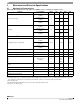
6 Register Descriptions Table 11. Register Address Map Name Type Register Address Auto-Increment Address F_READ=0 Default Hex Value F_READ=1 Comment STATUS(1)(2) R 0x00 00000000 0x00 Real time status OUT_X_MSB(1)(2) R 0x01 0x02 0x03 Output — [7:0] are 8 MSBs of 12-bit sample. OUT_X_LSB(1)(2) R 0x02 0x03 0x00 Output — [7:4] are 4 LSBs of 12-bit sample. OUT_Y_MSB(1)(2) R 0x03 0x04 0x05 Output — [7:0] are 8 MSBs of 12-bit sample.
Table 11. Register Address Map PULSE_THSZ(1)(3) R/W 0x25 0x26 00000000 0x00 (1)(3) R/W 0x26 0x27 00000000 0x00 Time limit for pulse PULSE_LTCY(1)(3) R/W 0x27 0x28 00000000 0x00 Latency time for 2nd pulse PULSE_WIND(1)(3) R/W 0x28 0x29 00000000 0x00 Window time for 2nd pulse (1)(3) PULSE_TMLT ASLP_COUNT Z pulse threshold R/W 0x29 0x2A 00000000 0x00 Counter setting for Auto-SLEEP (1)(3) R/W 0x2A 0x2B 00000000 0x00 ODR = 800 Hz, STANDBY Mode.
Table 12. STATUS Description ZYXOW X, Y, Z-axis Data Overwrite. Default value: 0 0: No data overwrite has occurred 1: Previous X, Y, or Z data was overwritten by new X, Y, or Z data before it was read ZOW Z-axis Data Overwrite. Default value: 0 0: No data overwrite has occurred 1: Previous Z-axis data was overwritten by new Z-axis data before it was read YOW Y-axis Data Overwrite.
Data Registers: 0x01 OUT_X_MSB, 0x02 OUT_X_LSB, 0x03 OUT_Y_MSB, 0x04 OUT_Y_LSB, 0x05 OUT_Z_MSB, 0x06 OUT_Z_LSB These registers contain the X-axis, Y-axis, and Z-axis 12-bit output sample data expressed as 2's complement numbers. The sample data output registers store the current sample data.
0x0C: INT_SOURCE System Interrupt Status Register In the interrupt source register the status of the various embedded features can be determined. The bits that are set (logic ‘1’) indicate which function has asserted an interrupt and conversely the bits that are cleared (logic ‘0’) indicate which function has not asserted or has deasserted an interrupt. The bits are set by a low to high transition and are cleared by reading the appropriate interrupt source register.
0x0D: WHO_AM_I Device ID Register The device identification register identifies the part. The default value is 0x2A. This value is factory programmed. Consult the factory for custom alternate values. 0x0D: WHO_AM_I Device ID Register (Read Only) Bit 7 Bit 6 Bit 5 Bit 4 Bit 3 Bit 2 Bit 1 Bit 0 0 0 1 0 1 0 1 0 0x0E: XYZ_DATA_CFG Register The XYZ_DATA_CFG register sets the dynamic range and sets the high pass filter for the output data. When the HPF_OUT bit is set.
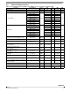
Table 18. High Pass Filter Cut-off Options Oversampling Mode = Normal SEL1 SEL0 800 Hz 400 Hz 200 Hz 100 Hz 50 Hz 12.5 Hz 6.25 Hz 1.56 Hz 0 0 16 Hz 16 Hz 8 Hz 4 Hz 2 Hz 2 Hz 2 Hz 2 Hz 0 1 8 Hz 8 Hz 4 Hz 2 Hz 1 Hz 1 Hz 1 Hz 1 Hz 1 0 4 Hz 4 Hz 2 Hz 1 Hz 0.5 Hz 0.5 Hz 0.5 Hz 0.5 Hz 1 1 2 Hz 2 Hz 1 Hz 0.5 Hz 0.25 Hz 0.25 Hz 0.25 Hz 0.25 Hz Oversampling Mode = Low Noise Low Power 0 0 16 Hz 16 Hz 8 Hz 4 Hz 2 Hz 0.5 Hz 0.5 Hz 0.
0x11 Portrait/Landscape Configuration Register This register enables the Portrait/Landscape function and sets the behavior of the debounce counter. 0x11 PL_CFG Register (Read/Write) Bit 7 Bit 6 Bit 5 Bit 4 Bit 3 Bit 2 Bit 1 Bit 0 DBCNTM PL_EN 0 0 0 0 0 0 Table 20. PL_CFG Description DBCNTM PL_EN Debounce counter mode selection. Default value: 1 0: Decrements debounce whenever condition of interest is no longer valid. 1: Clears counter whenever condition of interest is no longer valid.
0x14: P_L_THS_REG Portrait/Landscape Threshold and Hysteresis Register This register represents the Portrait to Landscape trip threshold. 0x14: P_L_THS_REG Register (Read Only) Bit 7 Bit 6 Bit 5 Bit 4 Bit 3 Bit 2 Bit 1 Bit 0 P_L_THS[4] P_L_THS[3] P_L_THS[2] P_L_THS[1] P_L_THS[0] HYS[2] HYS[1] HYS[0] : Table 24. P_L_THS_REG Description P_L_THS[7:3] HYS[2:0] Portrait/Landscape Fixed Threshold angle = 1_0000 (45°).
0x15 FF_MT_CFG Freefall/Motion Configuration Register This is the Freefall/Motion configuration register for setting up the conditions of the freefall or motion function. 0x15 FF_MT_CFG Register (Read/Write) Bit 7 ELE Bit 6 OAE Bit 5 ZEFE Bit 4 YEFE Bit 3 XEFE Bit 2 0 Bit 1 0 Bit 0 0 Table 26. FF_MT_CFG Description ELE Event Latch Enable: Event flags are latched into FF_MT_SRC register. Reading of the FF_MT_SRC register clears the event flag EA and all FF_MT_SRC bits. Default value: 0.
Table 27. Freefall/Motion Source Description EA ZHE ZHP YHE YHP XHE XHP Event Active Flag. Default value: 0. 0: No event flag has been asserted; 1: one or more event flag has been asserted. See the description of the OAE bit to determine the effect of the 3-axis event flags on the EA bit. Z Motion Flag. Default value: 0. 0: No Z Motion event detected, 1: Z Motion has been detected This bit reads always zero if the ZEFE control bit is set to zero Z Motion Polarity Flag. Default value: 0.
0x18 FF_MT_COUNT Debounce Register This register sets the number of debounce sample counts for the event trigger. 0x18 FF_MT_COUNT_Register (Read/Write) Bit 7 D7 Bit 6 D6 Bit 5 D5 Bit 4 D4 Bit 3 D3 Bit 2 D2 Bit 1 D1 Bit 0 D0 Table 29. FF_MT_COUNT Description D[7:0] Count value. Default value: 0000_0000 This register sets the minimum number of debounce sample counts of continuously matching the detection condition user selected for the freefall, motion event.
High g Event on all 3-axis (Motion Detect) Count Threshold (a) FF Counter Value FFEA High g Event on all 3-axis (Motion Detect) DBCNTM = 1 Count Threshold Debounce Counter Value (b) EA High g Event on all 3-axis (Motion Detect) DBCNTM = 0 Count Threshold Debounce Counter Value (c) EA Figure 14.
6.4 Transient (HPF) Acceleration Detection For more information on the uses of the transient function please review application note AN4071. This function is similar to the motion detection except that high pass filtered data is compared. There is an option to disable the high pass filter through the function. In this case the behavior is the same as the motion detection. This allows for the device to have 2 motion detection functions.
0x1F TRANSIENT_THS Register The Transient Threshold register sets the threshold limit for the detection of the transient acceleration. The value in the TRANSIENT_THS register corresponds to a g value which is compared against the values of High Pass Filtered Data. If the High Pass Filtered acceleration value exceeds the threshold limit an event flag is raised and the interrupt is generated if enabled.
6.5 Single, Double and Directional Tap Detection Registers For more details of how to configure the tap detection and sample code please refer to Freescale application note, AN4072. The tap detection registers are referred to as “Pulse”. 0x21: PULSE_CFG Pulse Configuration Register This register configures the event flag for the tap detection for enabling/disabling the detection of a single and double pulse on each of the axes.
0x23 - 0x25: PULSE_THSX, Y, Z Pulse Threshold for X, Y & Z Registers The pulse threshold can be set separately for the X, Y and Z axes. The PULSE_THSX, PULSE_THSY and PULSE_THSZ registers define the threshold which is used by the system to start the pulse detection procedure. 0x23 PULSE_THSX Register (Read/Write) Bit 7 0 Bit 6 THSX6 Bit 5 THSX5 Bit 4 THSX4 Bit 3 THSX3 Bit 2 THSX2 Bit 1 THSX1 Bit 0 THSX0 Bit 2 THSY2 Bit 1 THSY1 Bit 0 THSY0 Table 38.
Table 43. Time Step for PULSE Time Limit (Reg 0x0F) Pulse_LPF_EN = 0 ODR (Hz) Max Time Range (s) Time Step (ms) Normal LPLN HighRes LP Normal LPLN HighRes LP 800 0.159 0.159 0.159 0.159 0.625 0.625 0.625 0.625 400 0.159 0.159 0.159 0.319 0.625 0.625 0.625 1.25 200 0.319 0.319 0.159 0.638 1.25 1.25 0.625 2.5 100 0.638 0.638 0.159 1.28 2.5 2.5 0.625 5 50 1.28 1.28 0.159 2.55 5 5 0.625 10 12.5 1.28 5.1 0.159 10.2 5 20 0.625 40 6.25 1.28 5.1 0.
0x28 PULSE_WIND Register (Read/Write) 0x28: PULSE_WIND Second Pulse Time Window Register Bit 7 Bit 6 Bit 5 Bit 4 Bit 3 Bit 2 Bit 1 Bit 0 WIND7 WIND6 WIND5 WIND4 WIND3 WIND2 WIND1 WIND0 Table 47. PULSE_WIND Description WIND[7:0] Second Pulse Time Window. Default value: 0000_0000.
6.6 Auto-WAKE/SLEEP Detection The ASLP_COUNT register sets the minimum time period of inactivity required to change current ODR value from the value specified in the DR[2:0] register to ASLP_RATE register value, provided the SLPE bit is set to a logic ‘1’ in the CTRL_REG2 register. See Table 45 for functional blocks that may be monitored for inactivity in order to trigger the “return to SLEEP” event.
6.7 Control Registers Note: Except for STANDBY mode selection, the device must be in STANDBY mode to change any of the fields within CTRL_REG1 (0X2A). 0x2A: CTRL_REG1 System Control 1 Register 0x2A CTRL_REG1 Register (Read/Write) Bit 7 Bit 6 Bit 5 Bit 4 Bit 3 Bit 2 Bit 1 Bit 0 ASLP_RATE1 ASLP_RATE0 DR2 DR1 DR0 LNOISE F_READ ACTIVE Table 53. CTRL_REG1 Description ASLP_RATE[1:0] Configures the Auto-WAKE sample frequency when the device is in SLEEP Mode. Default value: 00.
0x2B: CTRL_REG2 System Control 2 Register 0x2B CTRL_REG2 Register (Read/Write) Bit 7 Bit 6 Bit 5 Bit 4 Bit 3 Bit 2 Bit 1 Bit 0 ST RST 0 SMODS1 SMODS0 SLPE MODS1 MODS0 Table 57. CTRL_REG2 Description Self-Test Enable. Default value: 0. 0: Self-Test disabled; 1: Self-Test enabled ST Software Reset. Default value: 0. 0: Device reset disabled; 1: Device reset enabled. RST SMODS[1:0] SLEEP mode power scheme selection. Default value: 00. See Table 58 and Table 59 Auto-SLEEP enable.
0x2C: CTRL_REG3 Interrupt Control Register 0x2C CTRL_REG3 Register (Read/Write) Bit 7 Bit 6 Bit 5 Bit 4 Bit 3 Bit 2 Bit 1 Bit 0 0 WAKE_TRANS WAKE_LNDPRT WAKE_PULSE WAKE_FF_MT 0 IPOL PP_OD Table 60. CTRL_REG3 Description WAKE_TRANS WAKE_LNDPRT WAKE_PULSE WAKE_FF_MT IPOL PP_OD 0: 1: 0: 1: Transient function is bypassed in SLEEP mode. Default value: 0. Transient function interrupt can wake up system Orientation function is bypassed in SLEEP mode. Default value: 0.
0x2E CTRL_REG5 Register (Read/Write) 0x2E: CTRL_REG5 Interrupt Configuration Register Bit 7 Bit 6 INT_CFG_ASLP 0 Bit 5 Bit 4 Bit 3 Bit 2 INT_CFG_TRANS INT_CFG_LNDPRT INT_CFG_PULSE INT_CFG_FF_MT Bit 1 Bit 0 0 INT_CFG_DRDY Table 62. Interrupt Configuration Register Description Interrupt Configuration Description INT1/INT2 Configuration. Default value: 0. 0: Interrupt is routed to INT2 pin; 1: Interrupt is routed to INT1 pin INT1/INT2 Configuration. Default value: 0.
Table 66.
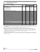
Table 67. Accelerometer Output Data 12-bit Data Range ±2g (1 mg) Range ±4g (2 mg) 0111 1111 1111 1.999g +3.998g Range ±8g (3.9 mg) +7.996g 0111 1111 1110 1.998g +3.996g +7.992g … … … … 0000 0000 0001 0.001g +0.002g +0.004g 0000 0000 0000 0.0000g 0.0000g 0.0000g 1111 1111 1111 -0.001g -0.002g -0.004g … … … … 1000 0000 0001 -1.999g -3.998g -7.996g 1000 0000 0000 -2.0000g -4.0000g -8.0000g 8-bit Data Range ±2g (15.6 mg) Range ±4g (31.25 mg) Range ±8g (62.
PACKAGE DIMENSIONS CASE 2077-01 ISSUE O 16-LEAD QFN MMA8452Q 44 Sensors Freescale Semiconductor
PACKAGE DIMENSIONS CASE 2077-01 ISSUE O 16-LEAD Q MMA8452Q Sensors Freescale Semiconductor 45
PACKAGE DIMENSIONS CASE 2077-01 ISSUE O 16-LEAD Q MMA8452Q 46 Sensors Freescale Semiconductor
How to Reach Us: Home Page: www.freescale.com Web Support: http://www.freescale.com/support USA/Europe or Locations Not Listed: Freescale Semiconductor, Inc. Technical Information Center, EL516 2100 East Elliot Road Tempe, Arizona 85284 1-800-521-6274 or +1-480-768-2130 www.freescale.