
Data Sheet


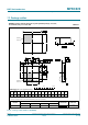


MFRC522 All information provided in this document is subject to legal disclaimers. © NXP Semiconductors N.V. 2016. All rights reserved.
Product data sheet
COMPANY PUBLIC
Rev. 3.9 — 27 April 2016
112139 84 of 95
NXP Semiconductors
MFRC522
Standard performance MIFARE and NTAG frontend
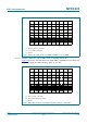
16.1.3.1 Example: Output test signals TestDAC1 and TestDAC2
The AnalogTestReg register is set to 11h. The output on pin AUX1 has the test signal
TestDAC1 and the output on pin AUX2 has the test signal TestDAC2. The signal values of
TestDAC1 and TestDAC2 are controlled by the TestDAC1Reg and TestDAC2Reg
registers.
Figure 28
shows test signal TestDAC1 on pin AUX1 and TestDAC2 on pin AUX2 when the
TestDAC1Reg register is programmed with a slope defined by values 00h to 3Fh and the
TestDAC2Reg register is programmed with a rectangular signal defined by values 00h
and 3Fh.
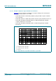
16.1.3.2 Example: Output test signals Corr1 and MinLevel
Figure 29
shows test signals Corr1 and MinLevel on pins AUX1 and AUX2, respectively.
The AnalogTestReg register is set to 24h.
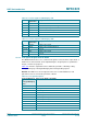
1101 RxActive
1110 subcarrier detected
1111 TstBusBit
Table 158. Test signal descriptions
…continued
AnalogSelAux1[3:0]
or
AnalogSelAux2[3:0]
value
Signal on pin AUX1 or pin AUX2
(1) TestDAC1 (500 mV/div) on pin AUX1.
(2) TestDAC2 (500 mV/div) on pin AUX2.
Fig 28. Output test signals TestDAC1 on pin AUX1 and TestDAC2 on pin AUX2
100 ms/div
001aak597
(1)
(2)