
Data Sheet


MFRC522 All information provided in this document is subject to legal disclaimers. © NXP Semiconductors N.V. 2016. All rights reserved.
Product data sheet
COMPANY PUBLIC
Rev. 3.9 — 27 April 2016
112139 83 of 95
NXP Semiconductors
MFRC522
Standard performance MIFARE and NTAG frontend
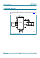
16.1.3 Test signals on pins AUX1 or AUX2
The MFRC522 allows the user to select internal signals for measurement on pins AUX1 or
AUX2. These measurements can be helpful during the design-in phase to optimize the
design or used for test purposes.
Table 158
shows the signals that can be switched to pin AUX1 or AUX2 by setting
AnalogSelAux1[3:0] or AnalogSelAux2[3:0] in the AnalogTestReg register.
Remark: The DAC has a current output, therefore it is recommended that a 1 k
pull-down resistor is connected to pin AUX1 or AUX2.
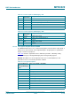
Table 156. Test bus signals: TestBusSel[4:0] = 07h
Pins Internal
signal name
Description
D6 s_data received data stream
D5 s_coll bit-collision detected (106 kBd only)
D4 s_valid s_data and s_coll signals are valid
D3 s_over receiver has detected a stop condition
D2 RCV_reset receiver is reset
D1 - reserved
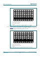
Table 157. Test bus signals: TestBusSel[4:0] = 0Dh
Pins Internal test
signal name
Description
D6 clkstable oscillator output signal
D5 clk27/8 oscillator output signal divided by 8
D4 to D3 - reserved
D2 clk27 oscillator output signal
D1 - reserved
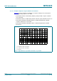
Table 158. Test signal descriptions
AnalogSelAux1[3:0]
or
AnalogSelAux2[3:0]
value
Signal on pin AUX1 or pin AUX2
0000 3-state
0001 DAC: register TestDAC1 or TestDAC2
0010 DAC: test signal Corr1
0011 reserved
0100 DAC: test signal MinLevel
0101 DAC: test signal ADC_I
0110 DAC: test signal ADC_Q
0111 to 1001 reserved
1010 HIGH
1011 LOW
1100 TxActive