
Data Sheet


MFRC522 All information provided in this document is subject to legal disclaimers. © NXP Semiconductors N.V. 2016. All rights reserved.
Product data sheet
COMPANY PUBLIC
Rev. 3.9 — 27 April 2016
112139 78 of 95
NXP Semiconductors
MFRC522
Standard performance MIFARE and NTAG frontend
[1] The voltage on pin RX is clamped by internal diodes to pins AVSS and AVDD.
[2] I
pd
is the total current for all supplies.
[3] I
DD(PVDD)
depends on the overall load at the digital pins.
[4] I
DD(TVDD)
depends on V
DD(TVDD)
and the external circuit connected to pins TX1 and TX2.
[5] During typical circuit operation, the overall current is below 100 mA.
[6] Typical value using a complementary driver configuration and an antenna matched to 40 between pins TX1 and TX2 at 13.56 MHz.
[7] I
DD(SVDD)
depends on the load at pin MFOUT.
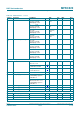
14.1 Timing characteristics
V
OH
HIGH-level output voltage pin OSCOUT - 1.1 - V
V
OL
LOW-level output voltage pin OSCOUT - 0.2 - V
C
i
input capacitance pin OSCOUT - 2 - pF
pin OSCIN - 2 - pF
Typical input requirements
f
xtal
crystal frequency - 27.12 - MHz
ESR equivalent series resistance - - 100
C
L
load capacitance - 10 - pF
P
xtal
crystal power dissipation - 50 100 mW
Table 153. Characteristics
…continued
Symbol Parameter Conditions Min Typ Max Unit
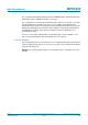
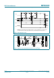
Fig 24. Pin RX input voltage range
001aak012
VMID
0 V
V
mod
V
i(p-p)(max)
V
i(p-p)(min)
13.56 MHz
carrier
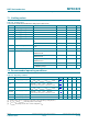
Table 154. SPI timing characteristics
Symbol Parameter Conditions Min Typ Max Unit
t
WL
pulse width LOW line SCK 50 - - ns
t
WH
pulse width HIGH line SCK 50 - - ns
t
h(SCKH-D)
SCK HIGH to data input
hold time
SCK to changing
MOSI
25 - - ns