
Data Sheet


MFRC522 All information provided in this document is subject to legal disclaimers. © NXP Semiconductors N.V. 2016. All rights reserved.
Product data sheet
COMPANY PUBLIC
Rev. 3.9 — 27 April 2016
112139 68 of 95
NXP Semiconductors
MFRC522
Standard performance MIFARE and NTAG frontend
9.3.4.10 TestDAC1Reg register
Defines the test value for TestDAC1.
9.3.4.11 TestDAC2Reg register
Defines the test value for TestDAC2.
9.3.4.12 TestADCReg register
Shows the values of ADC I and Q channels.
9.3.4.13 Reserved register 3Ch
Functionality reserved for production test.
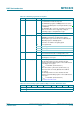
Table 135. TestDAC1Reg register (address 39h); reset value: xxh bit allocation
Bit 7 6 5 4 3 2 1 0
Symbol reserved TestDAC1[5:0]
Access - R/W
Table 136. TestDAC1Reg register bit descriptions
Bit Symbol Description
7 reserved reserved for production tests
6 reserved reserved for future use
5 to 0 TestDAC1[5:0] defines the test value for TestDAC1
output of DAC1 can be routed to AUX1 by setting value
AnalogSelAux1[3:0] to 0001b in the AnalogTestReg register
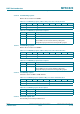
Table 137. TestDAC2Reg register (address 3Ah); reset value: xxh bit allocation
Bit 7 6 5 4 3 2 1 0
Symbol reserved TestDAC2[5:0]
Access - R/W
Table 138. TestDAC2Reg register bit descriptions
Bit Symbol Description
7 to 6 reserved reserved for future use
5 to 0 TestDAC2[5:0] defines the test value for TestDAC2
output of DAC2 can be routed to AUX2 by setting value
AnalogSelAux2[3:0] to 0001b in the AnalogTestReg register
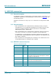
Table 139. TestADCReg register (address 3Bh); reset value: xxh bit allocation
Bit 7 6 5 4 3 2 1 0
Symbol ADC_I[3:0] ADC_Q[3:0]
Access R R
Table 140. TestADCReg register bit descriptions
Bit Symbol Description
7 to 4 ADC_I[3:0] ADC I channel value
3 to 0 ADC_Q[3:0] ADC Q channel value