
Data Sheet


MFRC522 All information provided in this document is subject to legal disclaimers. © NXP Semiconductors N.V. 2016. All rights reserved.
Product data sheet
COMPANY PUBLIC
Rev. 3.9 — 27 April 2016
112139 64 of 95
NXP Semiconductors
MFRC522
Standard performance MIFARE and NTAG frontend
9.3.4.3 TestSel2Reg register
General test signal configuration and PRBS control.
9.3.4.4 TestPinEnReg register
Enables the test bus pin output driver.
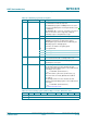
Table 120. TestSel1Reg register bit descriptions
Bit Symbol Description
7 to 3 reserved reserved for future use
2 to 0 TstBusBitSel
[2:0]
selects a test bus signal which is output at pin MFOUT
if AnalogSelAux2[3:0] = FFh in AnalogTestReg register, test bus signal
is also output at pins AUX1 or AUX2
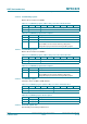
Table 121. TestSel2Reg register (address 32h); reset value: 00h bit allocation
Bit 7 6 5 4 3 2 1 0
Symbol TstBusFlip PRBS9 PRBS15 TestBusSel[4:0]
Access R/W R/W R/W R/W
Table 122. TestSel2Reg register bit descriptions
Bit Symbol Value Description
7 TstBusFlip 1 test bus is mapped to the parallel port in the following order:
TstBusBit4,TstBusBit3, TstBusBit2, TstBusBit6, TstBusBit5,
TstBusBit0; see Section 16.1 on page 82
6 PRBS9 - starts and enables the PRBS9 sequence according to ITU-TO150
Remark: all relevant registers to transmit data must be
configured before entering PRBS9 mode
the data transmission of the defined sequence is started by the
Transmit command
5 PRBS15 - starts and enables the PRBS15 sequence according to
ITU-TO150
Remark: all relevant registers to transmit data must be
configured before entering PRBS15 mode
the data transmission of the defined sequence is started by the
Transmit command
4 to 0 TestBusSel[4:0] - selects the test bus; see Section 16.1 “
Test signals”
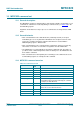
Table 123. TestPinEnReg register (address 33h); reset value: 80h bit allocation
Bit 7 6 5 4 3 2 1 0
Symbol RS232LineEn TestPinEn[5:0] reserved
Access R/W R/W -