
Data Sheet


MFRC522 All information provided in this document is subject to legal disclaimers. © NXP Semiconductors N.V. 2016. All rights reserved.
Product data sheet
COMPANY PUBLIC
Rev. 3.9 — 27 April 2016
112139 60 of 95
NXP Semiconductors
MFRC522
Standard performance MIFARE and NTAG frontend
9.3.3.8 CWGsPReg register
Defines the conductance of the p-driver output during periods of no modulation.
9.3.3.9 ModGsPReg register
Defines the conductance of the p-driver output during modulation.
9.3.3.10 TModeReg and TPrescalerReg registers
These registers define the timer settings.
Remark: The TPrescaler setting higher 4 bits are in the TModeReg register and the lower
8 bits are in the TPrescalerReg register.
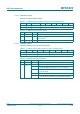
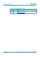
Table 101. CWGsPReg register (address 28h); reset value: 20h bit allocation
Bit 7 6 5 4 3 2 1 0
Symbol reserved CWGsP[5:0]
Access - R/W
Table 102. CWGsPReg register bit descriptions
Bit Symbol Description
7 to 6 reserved reserved for future use
5 to 0 CWGsP[5:0] defines the conductance of the p-driver output which can be used to
regulate the output power and subsequently current consumption and
operating distance
Remark: the conductance value is binary weighted
during soft Power-down mode the highest bit is forced to logic 1
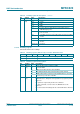
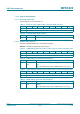
Table 103. ModGsPReg register (address 29h); reset value: 20h bit allocation
Bit 7 6 5 4 3 2 1 0
Symbol reserved ModGsP[5:0]
Access - R/W
Table 104. ModGsPReg register bit descriptions
Bit Symbol Description
7 to 6 reserved reserved for future use
5 to 0 ModGsP[5:0] defines the conductance of the p-driver output during modulation
which can be used to regulate the modulation index
Remark: the conductance value is binary weighted
during soft Power-down mode the highest bit is forced to logic 1
if the TxASKReg register’s Force100ASK bit is set to logic 1 the value
of ModGsP has no effect
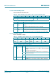
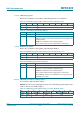
Table 105. TModeReg register (address 2Ah); reset value: 00h bit allocation
Bit 7 6 5 4 3 2 1 0
Symbol TAuto TGated[1:0] TAutoRestart TPrescaler_Hi[3:0]
Access R/W R/W R/W R/W