
Data Sheet


MFRC522 All information provided in this document is subject to legal disclaimers. © NXP Semiconductors N.V. 2016. All rights reserved.
Product data sheet
COMPANY PUBLIC
Rev. 3.9 — 27 April 2016
112139 59 of 95
NXP Semiconductors
MFRC522
Standard performance MIFARE and NTAG frontend
9.3.3.6 RFCfgReg register
Configures the receiver gain.
9.3.3.7 GsNReg register
Defines the conductance of the antenna driver pins TX1 and TX2 for the n-driver when the
driver is switched on.
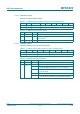
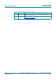
Table 97. RFCfgReg register (address 26h); reset value: 48h bit allocation
Bit 7 6 5 4 3 2 1 0
Symbol reserved RxGain[2:0] reserved
Access - R/W -
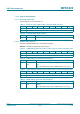
Table 98. RFCfgReg register bit descriptions
Bit Symbol Value Description
7 reserved - reserved for future use
6 to 4 RxGain
[2:0]
defines the receiver’s signal voltage gain factor:
000 18 dB
001 23 dB
010 18 dB
011 23 dB
100 33 dB
101 38 dB
110 43 dB
111 48 dB
3 to 0 reserved - reserved for future use
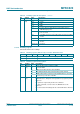
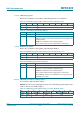
Table 99. GsNReg register (address 27h); reset value: 88h bit allocation
Bit 7 6 5 4 3 2 1 0
Symbol CWGsN[3:0] ModGsN[3:0]
Access R/W R/W
Table 100. GsNReg register bit descriptions
Bit Symbol Description
7 to 4 CWGsN
[3:0]
defines the conductance of the output n-driver during periods without
modulation which can be used to regulate the output power and
subsequently current consumption and operating distance
Remark: the conductance value is binary-weighted
during soft Power-down mode the highest bit is forced to logic 1
value is only used if driver TX1 or TX2 is switched on
3 to 0 ModGsN
[3:0]
defines the conductance of the output n-driver during periods without
modulation which can be used to regulate the modulation index
Remark: the conductance value is binary weighted
during soft Power-down mode the highest bit is forced to logic 1
value is only used if driver TX1 or TX2 is switched on