
Data Sheet


MFRC522 All information provided in this document is subject to legal disclaimers. © NXP Semiconductors N.V. 2016. All rights reserved.
Product data sheet
COMPANY PUBLIC
Rev. 3.9 — 27 April 2016
112139 52 of 95
NXP Semiconductors
MFRC522
Standard performance MIFARE and NTAG frontend
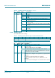
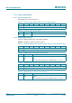
9.3.2.8 RxSelReg register
Selects internal receiver settings.
3 to 0 MFOutSel
[3:0]
selects the input for pin MFOUT
0000 3-state
0001 LOW
0010 HIGH
0011 test bus signal as defined by the TestSel1Reg register’s
TstBusBitSel[2:0] value
0100 modulation signal (envelope) from the internal encoder, Miller
pulse encoded
0101 serial data stream to be transmitted, data stream before Miller
encoder
0110 reserved
0111 serial data stream received, data stream after Manchester
decoder
1000 to 1111 reserved
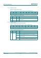
Table 66. TxSelReg register bit descriptions
…continued
Bit Symbol Value Description
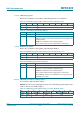
Table 67. RxSelReg register (address 17h); reset value: 84h bit allocation
Bit 7 6 5 4 3 2 1 0
Symbol UARTSel[1:0] RxWait[5:0]
Access R/W R/W
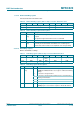
Table 68. RxSelReg register bit descriptions
Bit Symbol Value Description
7 to 6 UARTSel
[1:0]
selects the input of the contactless UART
00 constant LOW
01 Manchester with subcarrier from pin MFIN
10 modulated signal from the internal analog module, default
11 NRZ coding without subcarrier from pin MFIN which is only valid
for transfer speeds above 106 kBd
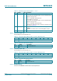
5 to 0 RxWait
[5:0]
- after data transmission the activation of the receiver is delayed for
RxWait bit-clocks, during this ‘frame guard time’ any signal on pin RX
is ignored
this parameter is ignored by the Receive command
all other commands, such as Transceive, MFAuthent use this
parameter
the counter starts immediately after the external RF field is switched
on