
Data Sheet


MFRC522 All information provided in this document is subject to legal disclaimers. © NXP Semiconductors N.V. 2016. All rights reserved.
Product data sheet
COMPANY PUBLIC
Rev. 3.9 — 27 April 2016
112139 50 of 95
NXP Semiconductors
MFRC522
Standard performance MIFARE and NTAG frontend
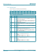
9.3.2.5 TxControlReg register
Controls the logical behavior of the antenna driver pins TX1 and TX2.
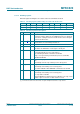
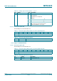
2 RxMultiple 0 receiver is deactivated after receiving a data frame
1 able to receive more than one data frame
only valid for data rates above 106 kBd in order to handle the
polling command
after setting this bit the Receive and Transceive commands will
not terminate automatically. Multiple reception can only be
deactivated by writing any command (except the Receive
command) to the CommandReg register, or by the host clearing
the bit
if set to logic 1, an error byte is added to the FIFO buffer at the
end of a received data stream which is a copy of the ErrorReg
register value. For the MFRC522 version 2.0 the CRC status is
reflected in the signal CRCOk, which indicates the actual status
of the CRC coprocessor. For the MFRC522 version 1.0 the CRC
status is reflected in the signal CRCErr.
1 to 0 reserved - reserved for future use
Table 60. RxModeReg register bit descriptions
…continued
Bit Symbol Value Description
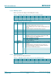
Table 61. TxControlReg register (address 14h); reset value: 80h bit allocation
Bit 7 6 5 4 3 2 1 0
Symbol InvTx2RF
On
InvTx1RF
On
InvTx2RF
Off
InvTx1RF
Off
Tx2CW reserved Tx2RFEn Tx1RFEn
Access R/W R/W R/W R/W R/W - R/W R/W
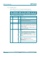
Table 62. TxControlReg register bit descriptions
Bit Symbol Value Description
7 InvTx2RFOn 1 output signal on pin TX2 inverted when driver TX2 is enabled
6 InvTx1RFOn 1 output signal on pin TX1 inverted when driver TX1 is enabled
5 InvTx2RFOff 1 output signal on pin TX2 inverted when driver TX2 is disabled
4 InvTx1RFOff 1 output signal on pin TX1 inverted when driver TX1 is disabled
3 Tx2CW 1 output signal on pin TX2 continuously delivers the unmodulated
13.56 MHz energy carrier
0 Tx2CW bit is enabled to modulate the 13.56 MHz energy carrier
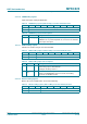
2 reserved - reserved for future use
1 Tx2RFEn 1 output signal on pin TX2 delivers the 13.56 MHz energy carrier
modulated by the transmission data
0 Tx1RFEn 1 output signal on pin TX1 delivers the 13.56 MHz energy carrier
modulated by the transmission data