
Data Sheet


MFRC522 All information provided in this document is subject to legal disclaimers. © NXP Semiconductors N.V. 2016. All rights reserved.
Product data sheet
COMPANY PUBLIC
Rev. 3.9 — 27 April 2016
112139 44 of 95
NXP Semiconductors
MFRC522
Standard performance MIFARE and NTAG frontend
9.3.1.10 FIFODataReg register
Input and output of 64 byte FIFO buffer.
9.3.1.11 FIFOLevelReg register
Indicates the number of bytes stored in the FIFO.
9.3.1.12 WaterLevelReg register
Defines the level for FIFO under- and overflow warning.
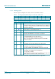
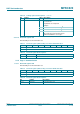
Table 39. FIFODataReg register (address 09h); reset value: xxh bit allocation
Bit 7 6 5 4 3 2 1 0
Symbol FIFOData[7:0]
Access D
Table 40. FIFODataReg register bit descriptions
Bit Symbol Description
7 to 0 FIFOData[7:0] data input and output port for the internal 64-byte FIFO buffer
FIFO buffer acts as parallel in/parallel out converter for all serial data
stream inputs and outputs
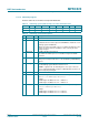
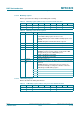
Table 41. FIFOLevelReg register (address 0Ah); reset value: 00h bit allocation
Bit 7 6 5 4 3 2 1 0
Symbol FlushBuffer FIFOLevel[6:0]
Access W R
Table 42. FIFOLevelReg register bit descriptions
Bit Symbol Value Description
7 FlushBuffer 1 immediately clears the internal FIFO buffer’s read and write pointer
and ErrorReg register’s BufferOvfl bit
reading this bit always returns 0
6 to 0 FIFOLevel
[6:0]
- indicates the number of bytes stored in the FIFO buffer
writing to the FIFODataReg register increments and reading
decrements the FIFOLevel value
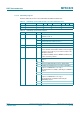
Table 43. WaterLevelReg register (address 0Bh); reset value: 08h bit allocation
Bit 7 6 5 4 3 2 1 0
Symbol reserved WaterLevel[5:0]
Access - R/W