
Data Sheet


MFRC522 All information provided in this document is subject to legal disclaimers. © NXP Semiconductors N.V. 2016. All rights reserved.
Product data sheet
COMPANY PUBLIC
Rev. 3.9 — 27 April 2016
112139 34 of 95
NXP Semiconductors
MFRC522
Standard performance MIFARE and NTAG frontend
The clock applied to the MFRC522 provides a time basis for the synchronous system’s
encoder and decoder. The stability of the clock frequency, therefore, is an important factor
for correct operation. To obtain optimum performance, clock jitter must be reduced as
much as possible. This is best achieved using the internal oscillator buffer with the
recommended circuitry.
If an external clock source is used, the clock signal must be applied to pin OSCIN. In this
case, special care must be taken with the clock duty cycle and clock jitter and the clock
quality must be verified.
8.8 Reset and oscillator start-up time
8.8.1 Reset timing requirements
The reset signal is filtered by a hysteresis circuit and a spike filter before it enters the
digital circuit. The spike filter rejects signals shorter than 10 ns. In order to perform a reset,
the signal must be LOW for at least 100 ns.
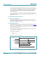
8.8.2 Oscillator start-up time
If the MFRC522 has been set to a Power-down mode or is powered by a V
DDX
supply, the
start-up time for the MFRC522 depends on the oscillator used and is shown in Figure 23
.
The time (t
startup
) is the start-up time of the crystal oscillator circuit. The crystal oscillator
start-up time is defined by the crystal.
The time (t
d
) is the internal delay time of the MFRC522 when the clock signal is stable
before the MFRC522 can be addressed.
The delay time is calculated by:
(8)
The time (t
osc
) is the sum of t
d
and t
startup
.
Fig 23. Oscillator start-up time
t
d
1024
27 s
--------------
37.74 s==
001aak596
t
startup
t
d
t
osc
t
device activation
oscillator
clock stable
clock ready