
Data Sheet

MFRC522 All information provided in this document is subject to legal disclaimers. © NXP Semiconductors N.V. 2016. All rights reserved.
Product data sheet
COMPANY PUBLIC
Rev. 3.9 — 27 April 2016
112139 25 of 95
NXP Semiconductors
MFRC522
Standard performance MIFARE and NTAG frontend
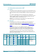
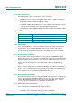
[1] X = Do not care.
The following abbreviations have been used in Table 15 and Table 16:
• RF: 13.56 MHz clock derived from 27.12 MHz quartz crystal oscillator divided by 2
• RF_n: inverted 13.56 MHz clock
• GSPMos: conductance, configuration of the PMOS array
• GSNMos: conductance, configuration of the NMOS array
• pCW: PMOS conductance value for continuous wave defined by the CWGsPReg
register
• pMod: PMOS conductance value for modulation defined by the ModGsPReg register
• nCW: NMOS conductance value for continuous wave defined by the GsNReg
register’s CWGsN[3:0] bits
• nMod: NMOS conductance value for modulation defined by the GsNReg register’s
ModGsN[3:0] bits
• X = do not care.
Remark: If only one driver is switched on, the values for CWGsPReg, ModGsPReg and
GsNReg registers are used for both drivers.
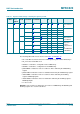
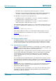
Table 16. Register and bit settings controlling the signal on pin TX2
Bit
Tx1RFEn
Bit
Force
100ASK
Bit
Tx2CW
Bit
InvTx2RFOn
Bit
InvTx2RFOff
Envelope Pin
TX2
GSPMos GSNMos Remarks
0X
[1]
X
[1]
X
[1]
X
[1]
X
[1]
X
[1]
X
[1]
X
[1]
not specified if
RF is switched
off
1000 X
[1]
0 RF pMod nMod -
1RFpCWnCW
1X
[1]
0 RF_n pMod nMod
1RF_npCWnCW
10 X
[1]
X
[1]
RF pCW nCW conductance
always CW for
the Tx2CW bit
1X
[1]
X
[1]
RF_n pCW nCW
100 X
[1]
0 0 pMod nMod 100 % ASK: pin
TX2 pulled
to logic 0
(independent of
the
InvTx2RFOn/Inv
Tx2RFOff bits)
1RFpCWnCW
1X
[1]
0 0 pMod nMod
1RF_npCWnCW
10 X
[1]
X
[1]
RF pCW nCW
1X
[1]
X
[1]
RF_n pCW nCW