
Data Sheet


MFRC522 All information provided in this document is subject to legal disclaimers. © NXP Semiconductors N.V. 2016. All rights reserved.
Product data sheet
COMPANY PUBLIC
Rev. 3.9 — 27 April 2016
112139 20 of 95
NXP Semiconductors
MFRC522
Standard performance MIFARE and NTAG frontend
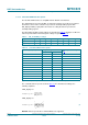
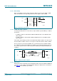
8.1.4.7 Register read access
To read out data from a specific register address in the MFRC522, the host controller must
use the following procedure:
• Firstly, a write access to the specific register address must be performed as indicated
in the frame that follows
• The first byte of a frame indicates the device address according to the I
2
C-bus rules
• The second byte indicates the register address. No data bytes are added
• The Read/Write bit is 0
After the write access, read access can start. The host sends the device address of the
MFRC522. In response, the MFRC522 sends the content of the read access register. In
one frame all data bytes can be read from the same register address. This enables fast
FIFO buffer access or register polling.
The Read/Write (R/W) bit is set to logic 1.
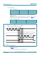
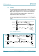
Fig 17. Register read and write access
001aak592
SA00
I
2
C-BUS
SLAVE ADDRESS
[A7:A0]
JOINER REGISTER
ADDRESS [A5:A0]
write cycle
0
(W)
A
DATA
[7:0]
[0:n]
[0:n]
[0:n]
A
P
SA00
I
2
C-BUS
SLAVE ADDRESS
[A7:A0]
JOINER REGISTER
ADDRESS [A5:A0]
read cycle
optional, if the previous access was on the same register address
0
(W)
A
P
P
S
S start condition
P stop condition
A acknowledge
A not acknowledge
W write cycle
R read cycle
A
I
2
C-BUS
SLAVE ADDRESS
[A7:A0]
sent by master
sent by slave
DATA
[7:0]
1
(R)
A
DATA
[7:0]
A